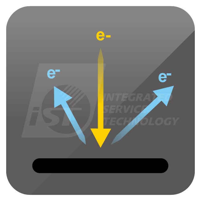
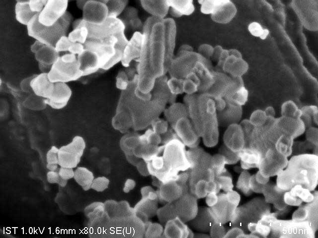
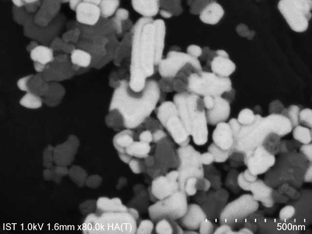
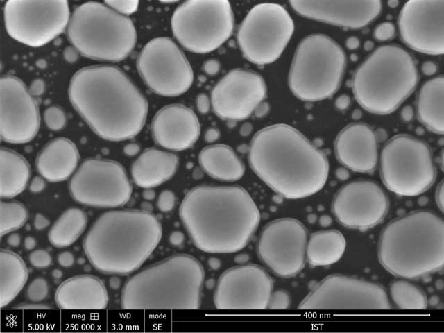
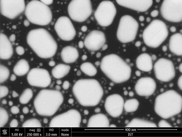
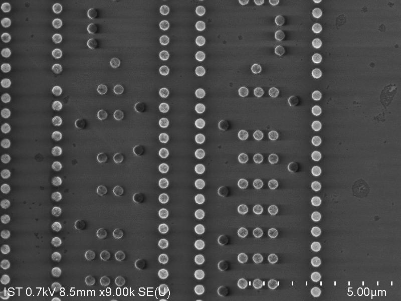
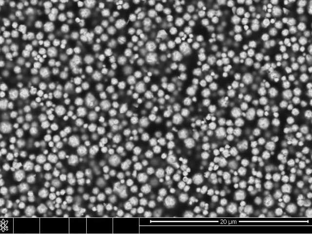
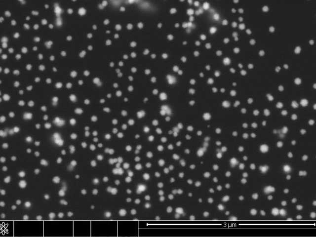
The Scanning Electron Microscope (SEM) uses optoelectronic system to focus electrons generated by an electronic gun onto a small spot on the sample surface. This beam of electrons will then interact with the sample material to generate secondary electrons, back scatter and signature X-Ray etc. A scan coil is then placed on sample surface to pick up those signals. The SEM works by collecting secondary electrons to form an image.
The Superiority of iST
iST has multiple main stream Field-Emission SEM (FE-SEM):Hitachi SU8600、Hitachi Regulus 8240、Hitachi SU8220、Hitachi SU8020 all equipped with EDS (SDD detector). Apart from providing the high resolution surface structure image, they are also capable of material composition analysis at a rapid pace. Additionally, they are equipped with a YAG BSE Detector, allowing the SEM to use backscattered electrons (BSE) for imaging.
Case Sharing
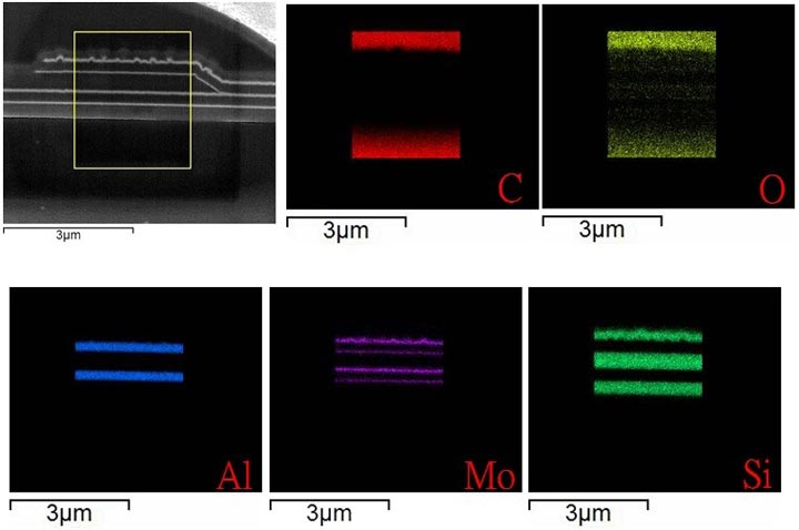
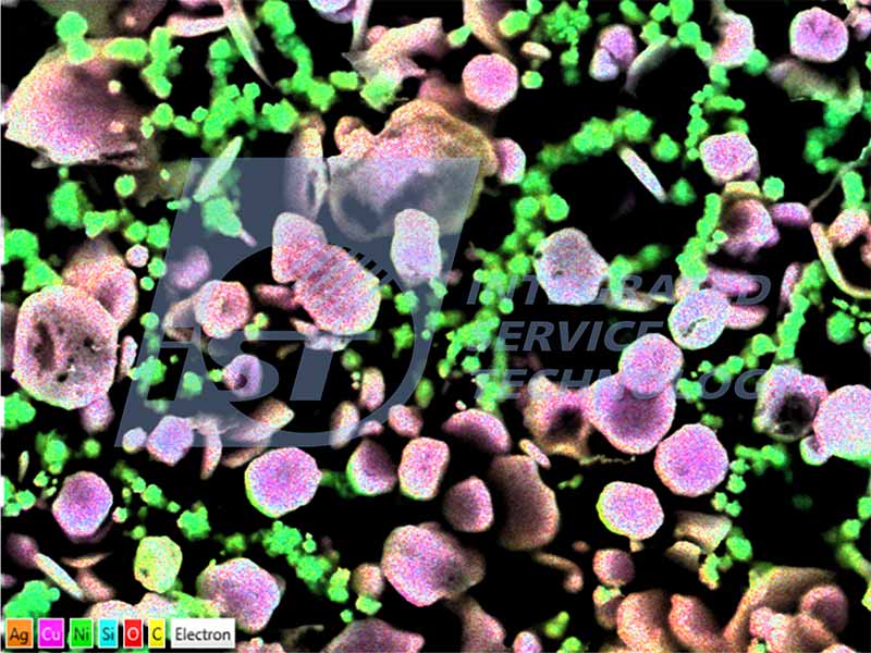
The element distribution status of liquid material and silver paste can be confirmed using EDS mapping
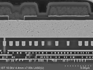
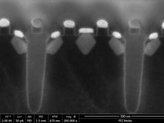
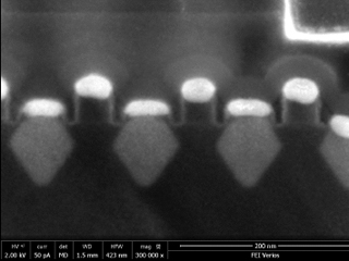
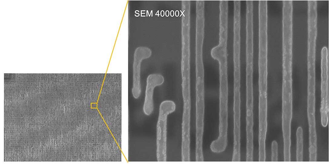
This chip image by SEM; the one on the left side is mosaicked with 100 SEM photos; the one on the right is an enlarged part from the left which shows the nano-grade circuit image clearly.
With stacked delayer and SEM photo stitching, customers may view the relationship between individual metal layers with iST software.
- Observation of material’s surface micro structure.
- It is possible to provide precise dimensional measurement such as film thickness
- EDS can provide qualitative or semi-qualitative element analysis of the surface sample as well as point, line scan or mapping analysis of the specified region
- The SDD detector can even improve the Mapping of spatial resolution under low voltage.
- SEM imaging with layer removal technique (de-process) can provide useful clue for reverse engineering of electrical circuits.
- Using low energy electron beam for Passive Voltage Contrast (PVC) can point out the precise location of electrical leakage or bad contact.
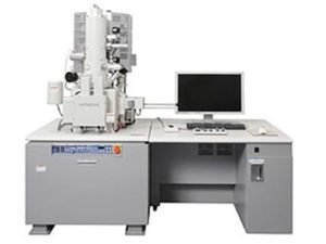
HITACHI SU8020
- Electron gun:Cold FE
- Resolution:1.0nm (accelerating voltage15kV) ,1.3nm(accelerating voltage 1kV)
- Magnification:30~800k
- Accelerating voltage:0.1~30kV
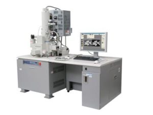
HITACHI SU8220
- Electron gun:Cold FE
- Resolution:0.8nm (accelerating voltage15kV) ,1.1nm(accelerating voltage1kV)
- Magnification:20~1000k
- Accelerating voltage:0.01~30kV
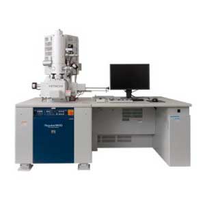
HITACHI Regulus 8240
- Electron gun: Cold FE
- Resolution: 0.7nm (accelerating voltage 15kV), 0.9nm (accelerating voltage 1kV)
- Magnification:20~1000k
- Accelerating voltage:0.01~30kV
- Auto Capture
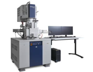
HITACHI SU8600
- Electron gun: Cold FE
- Resolution: 0.6nm (accelerating voltage 15kV), 0.7nm (accelerating voltage 1kV)
- Magnification:20~1000k
- Accelerating voltage:0.01~30kV
Contact Window | Ms. Yang/Cindy | Tel:+886-3-5799909#6641 | Email:web_pfa@istgroup.com

