
TEM (Transmission Electron Microscopy/Microscope) analyzes material microstructure and lattice defects. Imaging ultra-thin samples with high-energy electron beams yields 0.1nm resolution.
At iST, we understand that accurate TEM analysis requires careful TEM sample preparation. The accuracy of microscopic pictures and the validity of the obtained data depend on this step. It demonstrates that sample preparation immediately affects TEM findings. We optimize the preparation of various kinds of inorganic solid state samples, especially semiconductor materials and devices using Dual-beam FIB-SEM for ultra-thin lamella formation, and plasma cleaning for contamination removal and reducing carbon contamination during TEM observation.
In addition, we use low-energy ion milling to reduce amorphization, which maintains samples that are vulnerable to beam damage. We use these contemporary techniques to provide our customers with the best TEM tests while focusing on sample integrity and resolution.
Criticality of Sample Preparation
Importance of Precision in TEM Sample Preparation
We recommend rigorous TEM sample preparation because the sample’s structural and chemical composition affects TEM analysis clarity, resolution, and accuracy. Semiconductor samples of different types of structures and different patterns need different preparation processes to retain their original condition or emphasize specific properties. For instance, beam-sensitive materials need low-energy ion milling before examination for their inherent characteristics.
Material-Specific Preparation Techniques
Given the diverse nature of the samples we encounter, we customize TEM sample preparation methods depending on material properties and desired information. Electropolishing or ion milling metals creates thin, electron-transparent samples without artifacts. On the other hand, semiconductor samples with the surface layer terminated at different manufacturing processes need different protection techniques to prevent damage during the FIB cutting procedure. Preparation methods must be adaptable for meaningful TEM findings since they may influence the sample’s electron transparency and surface consistency.
Outcome Influences Through Preparation Techniques
Furthermore, the initial preparation techniques might also affect TEM analysis results. For example, preparing a local electrode atom probe (LEAP) permits nanoscale site-specific interface investigation in semiconductor devices. Meanwhile, site-specific cross-sections prepared by focused ion beam (FIB) milling may expose interior structures with minimum artifacts for defect investigation and material characterization. TEM sample preparation must be adjusted to elicit particular insights from complicated materials.
Integration with Advanced Technologies
Sophisticated TEM sample preparation technologies, including DualBeam FIB-SEM systems, help us generate high-quality samples with exact thickness and surface smoothness. The integration allows site-specific lamellae for in-situ experiments to study material behavior under different situations. These precise methods guarantee samples reflect the genuine material state for high-resolution Transmission Electron Microscopy (HRTEM) investigation.
Continuous Innovation in Sample Preparation
To handle material complexity and TEM analysis depth, iST continually innovates its TEM sample preparation methods and workflows. Automation and current imaging software expedite preparation while decreasing accidental mistakes and increasing throughput without compromising quality. Our attention to TEM sample preparation procedures underlines that we support groundbreaking scientific research and development across disciplines.
Overview of the TEM Sample Preparation Process
- Identifying the Material: TEM sample preparation begins with material selection as per the characteristics and information required. It meets TEM analysis standards.
- Choosing the Right Tools: For TEM sample preparation, we utilize DualBeam FIB-SEM technology for material removal and site-specific sample preparation.
- Initial Sample Protection: Initially, we use thin film techniques, such as sputtering or ALD, to coat the specimen with a layer of thin film to maintain the original morphology and to protect the top surface of a semiconductor device from being damaged by following FIB cutting.
- Mounting the Sample: Mounting the sample on a suitable holder offers stability during sample preparation. Proper mounting improves imaging focus and orientation.
- Thinning the Sample: With FIB milling, we thin the sample to electron transparency. We control the ion beam to avoid sample damage and give uniform thickness.
- Polishing to Remove Damage: We polish the sample using low-energy ion milling to lower surface damage. It enhances sample integrity for high-resolution TEM analysis.
- Plasma Clean: After being loaded into the specimen holder, the TEM specimen with the holder is cleaned by plasma to clean the surface of the TEM specimen. Plasma clean also helps to minimize carbon contamination during TEM analysis.
- Loading into TEM: Carefully, we load the prepared sample into the TEM. Remember, proper loading techniques preclude sample damage and misalignment.
- Adjusting TEM Settings: Finally, we adjust the TEM settings for the specific sample characteristics. This adjustment helps attain high-quality TEM images and data.
What Can iST Do For You?
For customer demands, iST uses modern TEM technology to analyze fine structures, crystalline flaws, and chemical compositions at atomic sizes. With 24/7 dual-shift operation, our market-leading TEM analysis reaches the 2nm technology node for fast findings. Both FEI and JEOL TEM equipment and Thermo Fisher Scientific's Helios Dual-beam FIB for TEM sample preparation are available. This setting lowers sample damage and produces quality TEM data. We provide accuracy in microstructure, defect, composition, stress, and other analysis services for semiconductors, LED, optoelectronics, and MEMS industries.
Hence, our creative TEM sample preparation services boost your research. We prepare your samples for transmission electron microscopy using cutting-edge tools and experience, which provides unmatched insights into your materials' structure and properties. Our simplified process saves time and effort, letting you concentrate on essential breakthroughs. Discover our offerings now and further your research with accuracy and convenience!

The Superiority of iST
Case Sharing
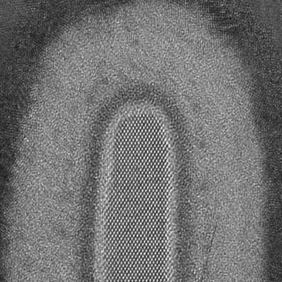
High resolution atom image
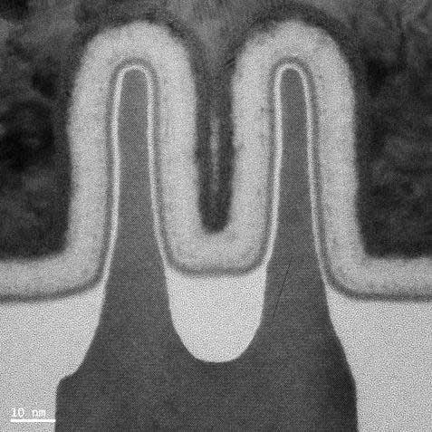
Advanced process FINFET image
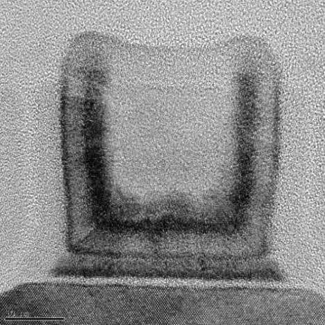
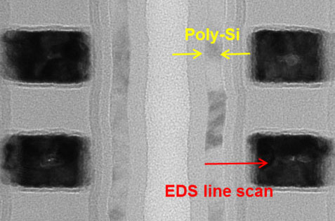
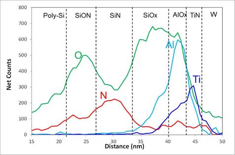
28nm HKMG transistor TEM image
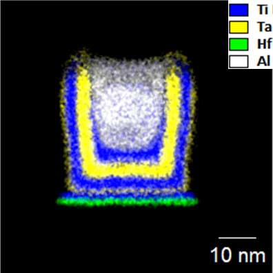
28nm HKMG transistor EDS mapping
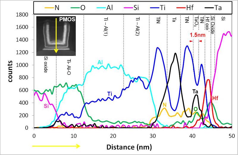
28 nm HKMG Transistor EDS line-scan
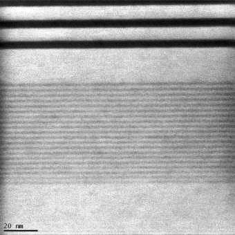
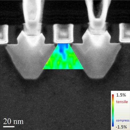
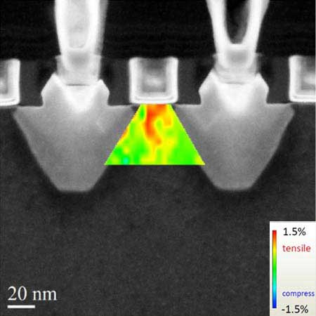
3D V-NAND Flash structure analysis
3D V-NAND Flash EDS line scan Analysis
LED QW and N spacer epitaxy structure
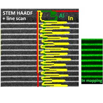
EDS elemental analysis of LED QW structure
Horizontal direction
Vertical direction
- Micro structure analysis (lattice image).
- Crystalline defect analysis.
- Element ingredient analysis.
- Thin film stress analysis.
- Electron diffraction analysis.
- Impurity and pollutant analysis.
- Auto Metrology Analysis.
- Semiconductor industry
- LED industry
- Optoelectronics industry
- MEMS industry
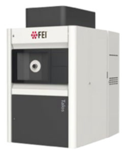
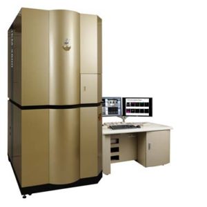
FEI Talos-F200
| Image | TEM resolution: 0.1nm STEM resolution: 0.16nm |
| EDS | Detector: SDD 30 mm2 x 4 Solid angle: 0.95 |
| Other functions | Piezo stage + DCFI 4K x 4K CCD |
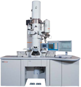
JEOL JEM-2800F
| Image | TEM resolution: 0.1nm STEM resolution: 0.2nm |
| EDS | Detector: SDD 100 mm2 x 2 Solid angle: 1.7 |
| Other functions | Strain mapping 4K x 4K CCD |
JEOL JEM-2100F
| Image | TEM resolution: 0.1nm STEM resolution: 0.2nm |
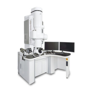
JEOL JEM-F200
| Image | TEM resolution: 0.1nm STEM resolution: 0.16nm |
| EDS | Detector: SDD 100 mm2 x 2 Solid angle: 1.7 |
| Other functions | Strain mapping 4K x 4K CCD |
Contact Window | Dr. Lin/Weijui | Tel:+886-3-5799909#6166 | Email:web_ma@istgroup.com