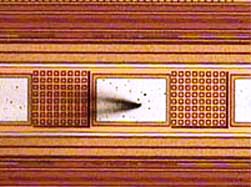
Beneath the Optical Microscope (OM) and Scanning Electron Microscope (SEM), probes are connected to internal circuits of an IC, allowing connection with external devices for inputting signals or conducting electrical measurements.
The Superiority of iST
Case Sharing
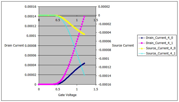
Vgs vs. Ids curve:
When fixing Vds of a transistor, Ids varies when Vgs changes, forming a “Vgs vs. Ids” curve.
This curve can be used for studying how the carriers (electrons or “electric holes”) in the channel are raised to the conducting zone. Both the critical voltage at which a channel is formed and the critical voltage of a linear zone can be measured, providing important curves for the study of transistor characteristics.
- Electrical Analysis Of Devices
- Study Of MEMS(Micro Electro Mechanical System) And Micro-Structured IC
- May Be Applied In High-Frequency Circuit And FIB Probing PAD And Active Probe (500 MHz)
- Probes May Be Employed To Provide Signal Input And Output In Case Sample Test Requiring Instruments Like EMMI / OBIRCH / TLP / ESD / Curve Tracer Yet Without Proper Jig
- Wafers May Subject To Individual Tests With This Probe Pad
- The Lab Is Equipped With A Laser System For Laser Cutting
Contact Window | Mr. Lin/Encheng | Tel:+886-3-5799909#6773 | Email:web_EFA@istgroup.com


