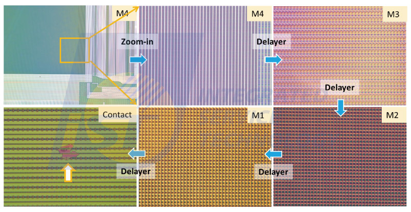
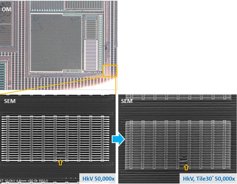
Remove the multi-layer structure of the chip (passivation, metal, Oxide) by repetitive combination of different approaches (ion etching/ chemical etching/ mechanical polishing), to enable clearly presenting circuit layout structure of each layer for later experiments.
The Superiority of iST
Case Sharing
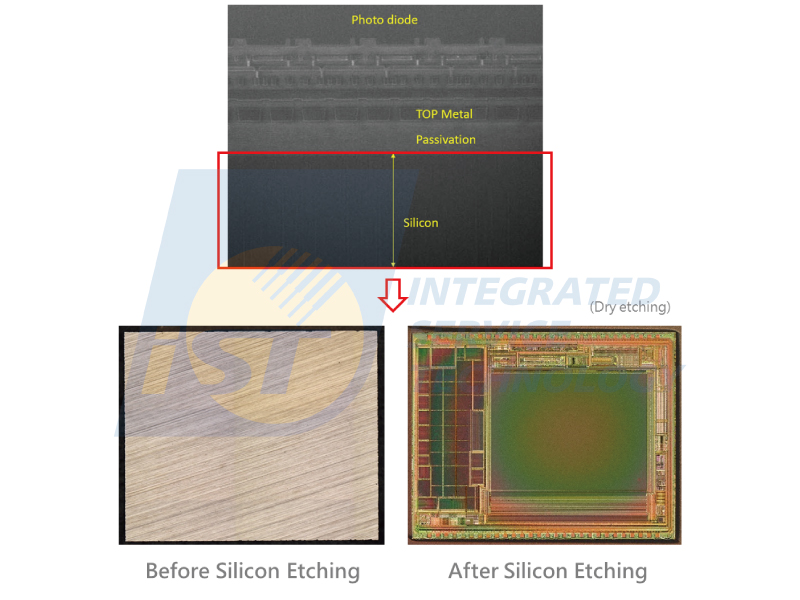
First step, silicon layer was etching to expose top metal layer for BSI .
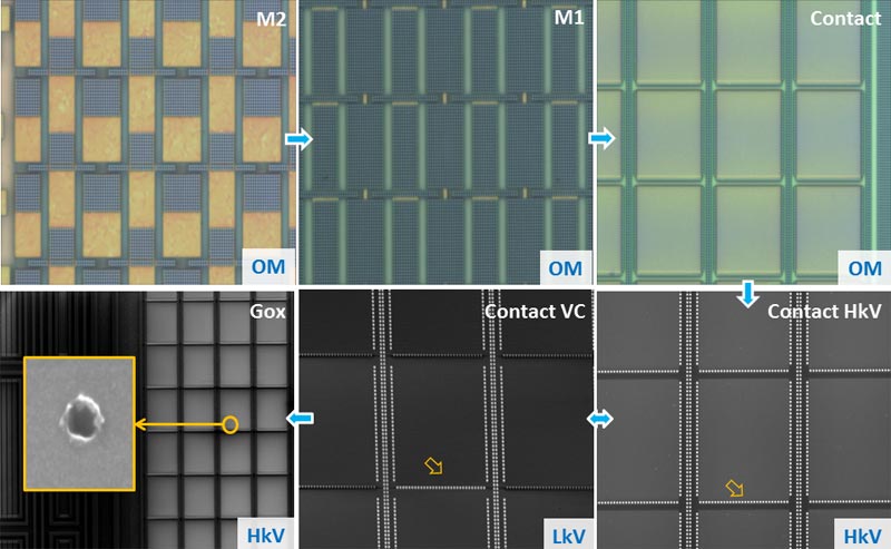
Using polish/dry etching/wet dry ways to delayer from top metal to contact layer. Using OM/SEM to inspect abnormality on each layer. Abnormality was observed on contact layer.
IC delayer → OM reviewing → Contact layer scanning (VC) with SEM high and low voltage→ etching to gate oxide then view by SEM
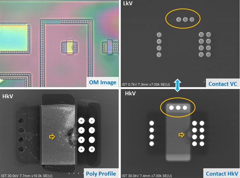
IC delayer to Contact → OM viewing and imaging →SEM electronic and secondary electronic scanning → polishing to poly → SEM scanning to get Poly Profile
FinFET process delayer to Substrate → OM viewing and imaging →SEM scanning
Contact Window | Mr. Ho/Rejo | Tel:+886-3-5799909#6795 | Email:web_decap@istgroup.com