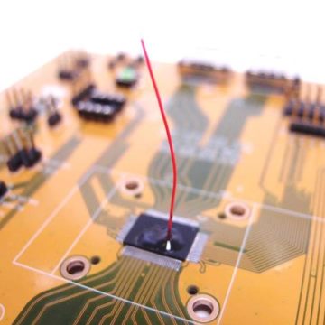
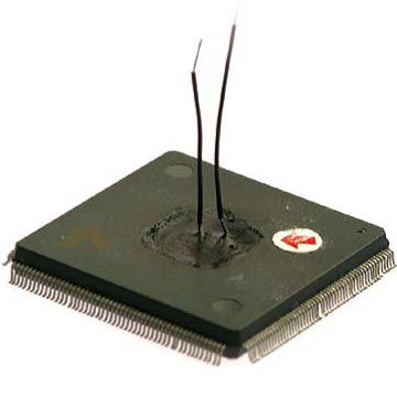
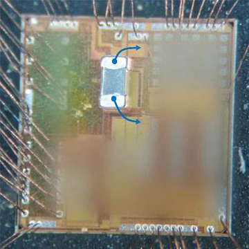
Conductive holes and pads are formed on the IC surface by way of FIB, and then they are connected with metal wires through special bonding to form conductive paths.
The Superiority of iST
| Superiority Comparison | N-FIB | Conventional FIB |
|---|---|---|
| R esistance with long wiring (1000 μ m) | 1 Ω± 10% | 7000 Ω± 10% |
| Parasitic capacitance | < 200fF | Less |
| Parasitic inductance | ~0.5nH/mm | Less |
| Current limit | Less | Possible |
| Power line | 1A | 3mA |
| Insert device | Yes | No |
Contact Window | Mr. Wang/Chino | Tel: +886-3-5799909#6000 | Email: web_fib@istgroup.com


