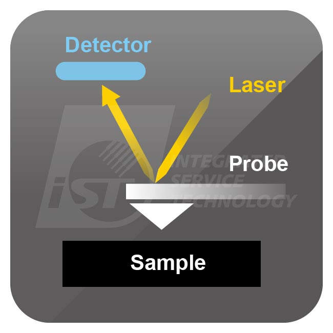
The main principle of AFM is to cause a micro displacement of the cantilever (which carries the probe) using the atomic forces between the probe tip and the sample, to map the topography of the sample. AFM is applicable to various material surface inspections.
What can iST do for you
AFM gives atom-scale resolution, forming a key means for studying surface of micro structures.

The Superiority of iST
- A 12" wafer containable AFM machine is rare within Taiwan and mainland industry. This enables analysis without breaking the wafer and maintains its completeness for later tests.
- The NX-Wafer atomic force profilometry has the largest scan area in industry accompany with excellent image resolution.
- The extra microscope with additional functions enables a still wider scope of analysis applications, i.e., CAFM (Conductive Atomic Force Microscopy) and SCM (Scanning Capacitance Microscopy).
| AFM | AFM profiler | CAFM | SCM | |
|---|---|---|---|---|
| Analysis mechanism | Measure the surface structure and looks by atomic forces between the probe tip and sample | The probe applies voltage on its tip or sample to get the current strength at the sample surface | Get the differential of capacitance signals with a conductive probe, convert them into 2D doping image distribution | |
| Analysis application | 1. Material surface roughness measurement and structure observation 2. Material surface 2D/3D pattern image 3. Nanoscale depth analysis and dimensioning | 1. Detect over resistance or current leakage 2. Identify P+/ N+ /Poly contact 3. Measure single point I-V curve | P-N type zone and border | |
| Equipment specification | 1. Sample dimension: (mm) 200 x 200 x 15 2. 300 mm x 300 mm (12" wafer) Compatible 3. Analysis scope (um): 90 x 90 x 5 | 1. Sample dimension:300 mm x 300 mm (12" wafer) Compatible 2. Maximun scanning range:50000 um | 1. Magnification ratio: 107~1011 2. Bias voltage range: -10V~10V | 1. Plane resolution: 20nm Doping concentration 2. Range: 1015~1019 atom/cm3 3. Scanning range: 90 * 90um / with height in 2cm |
Case Sharing
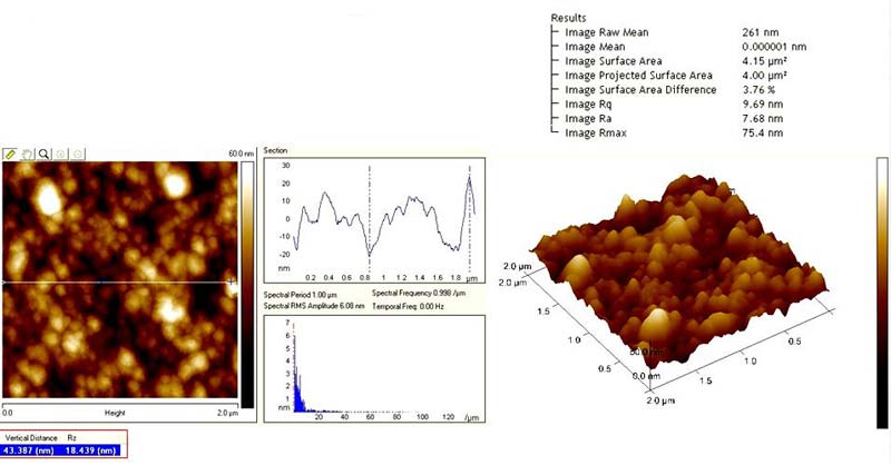
Get SAD percentage, Rq and Ra values based on 2D and 3D surface roughness analysis chart
The maximun 50000 um long range profiler with atomic resolution can provide the details of surface topography and roughness information.
Surface looks after AFM analysis
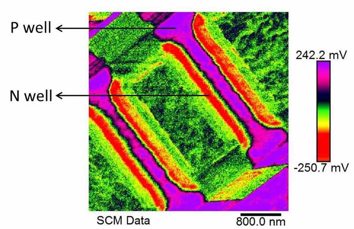
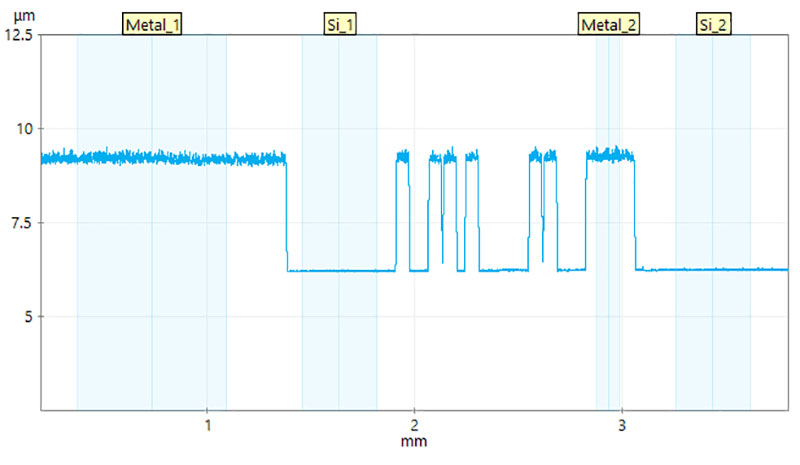
Determine the P/N well location by SCM
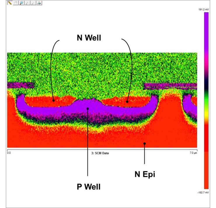
Determine the N Well / P Well /N Epi layer location by SCM
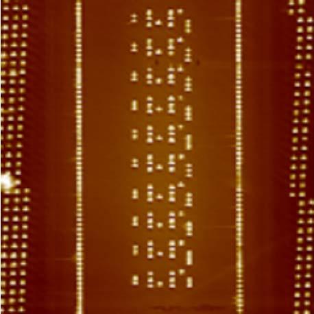
Contact VC with positive voltage (+1v) applied (no hot spot occurs)
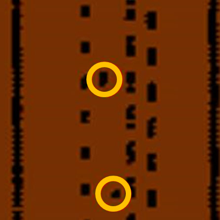
Contact VC with negative voltage (-1v) applied (hot spot occurs)
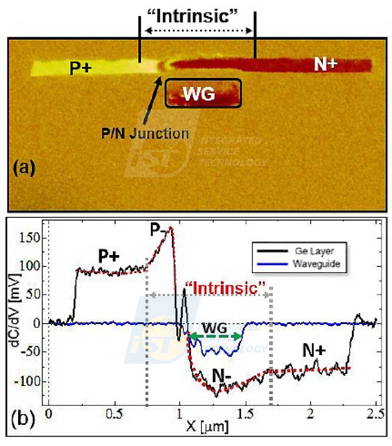
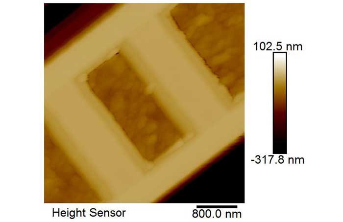
The changes in the depletion width (Wd) can be observed through SCM.
Image source:978-1-5386-4513-0/18 ©2018 IEEE
- Membrane roughness tests
- Structural study of micro surfaces
- 2D/3D material surface topography
- Nanoscale step height analysis
- Depletion Analysis in Silicon Photonic Devices
Bruker Dimension Icon
Bruker INNOVA
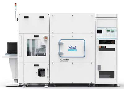
Park System NX-Wafer
Contact Window | Ms. Wu/Ping | Tel:+886-3-5799909#6183 | Email:web_ma@istgroup.com