Issued Date:2023/12/5 GaN defect
Issued By:iST
In the world of wide bandgap semiconductors, a significant breakthrough is underway. How can we overcome failure analysis bottlenecks to identify defects in high-power GaN chips with their unique structural challenges?
GaN defect

Wide Bandgap semiconductors, such as Gallium Nitride (GaN) and Silicon Carbide (SiC), have gained popularity in recent years. They are also known as the compound semiconductors.
Compared to traditional first-generation semiconductors (ex: Silicon) and second-generation semiconductors (ex: GaAs, InP), wide bandgap semiconductors are widely employed in power components due to their wide bandgap, low leakage, high voltage and temperature tolerance. Moreover, they offer better energy conversion efficiency. GaN, for instance, can support higher switching frequencies and provide excellent power density. They reduce the overall system size effectively for the same electrical performance. GaN is typically used in medium-power products with medium voltage (50V to 900V). On the other hand, SiC are suitable for high-power applications with high voltage (1,000V and above).
Taking GaN transistors as an example, they are now widely used in the fast-charging market of consumer electronics such as smartphones and laptops. Additionally, the rapid growth in demand for data centers has become another significant application area for GaN transistors. Furthermore, with the global trend of phasing out gasoline cars, applications like On-Board Chargers (OBC) and Electric Vehicle DC-DC converters are expected to showcase the excellence of GaN transistors. This trend indicates that GaN transistors are not only becoming a focal point for numerous automobile manufacturers but are also gradually revealing their extensive market potential.
In this edition of iST Classroom, we will first introduce the two main structures of power transistors and then delve into how iST’s unique solution can be used to localize defects in GaN transistor chips. This process effectively enhances the chances of pinpointing defects during physical failure analysis. It helps eliminate the frustration of not being able to identify defects, accelerating product validation and improving yield effectively.
GaN defect
GaN defect
1. Introduction to Two Major Power Transistor Structures
The commonly used power transistor structures today can be broadly categorized into two major types: (1) Vertical Structure and (2) Horizontal Structure.
(1) Vertical Structure
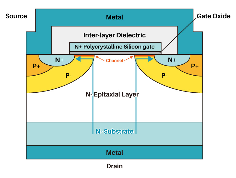
Figure 1: Schematic diagram of a vertical power MOSFET structure
(Source: A Review on Power MOSFET Device Structures, International Journal of Applied Science and Engineering, 2017)The common Vertical Double-diffused MOSFET (VDMOS) widely used in both Si (Silicon) and SiC (Silicon Carbide). In this structure, the current path follows the green line as depicted in Figure 1. To enhance its electrical characteristics, techniques like utilization of special trench gate designs and wafer thickness reduction are commonly used.
(2) Horizontal Structure
Lateral Double-diffused MOSFET (LDMOS) are commonly used in silicon-based transistors. The GaN High Electron Mobility Transistors (HEMTs) that this article focuses on, which also utilize the LDMOS structure. The schematic diagram is shown in Figure 2.
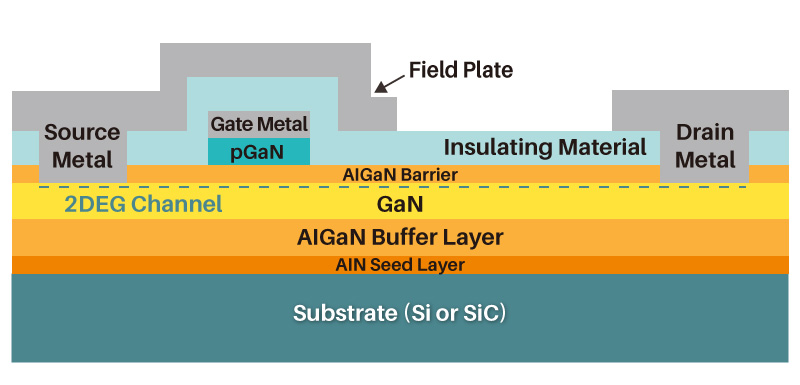
Figure 2: Schematic diagram of GaN HEMT horizontal structure
(Source:Lidow, A., Beach, R., Nakata, A., Cao, J., and Zhao, G.Y. (2013). US Patent 8,404,508, 26 March 2013.)The current market mainstream is the GaN-on-Si structure. This structure utilizes processes involving GaN epitaxy and metal interconnections to place the P-doped GaN gate, source and drain onto a Si Substrate. This structure offers the following advantages:
- Compatibility with standard silicon wafer processes, making it cost-effective and flexible for high-volume production in typical wafer fabs with idle capacity.
- The 2-Dimensional Electron Gas (2DEG) is formed at the hetero-interface between GaN and AlGaN. It has very high charge density and mobility, which can effectively reducing RDS(on) and improving component operating speed.
- By employing P-type GaN to deplete 2DEG, the normally open mode (Normally Open) device is transformed into an enhanced mode of Normally Off, similar to the driving method of Si MOSFET. This makes it more user-friendly for designers.
- This gate oxide-free structure provides high gate reliability.
2. Differences in Failure Analysis Between GaN and Conventional Silicon Components
For GaN chip structures near gate area, the designs are relatively complex. Different forms of Field Plate (FP) designs are typically used to reduce peak electric fields and interface traps. Additionally, the use of the top Redistribution Layer (RDL) in the chip’s design optimizes its electrical characteristics. As in general failure analysis, it is essential to measure I-V curves to understand the chip’s abnormal electrical characteristics before proceeding with destructive analysis. Parameters such as Drain-source Saturation Current (IDSS), Gate-Source Leakage Current (IGSS), or functional testing should be employed to confirm the conditions of electrical abnormalities, followed by further hot spot analysis in order to pinpoint the defect area.
However, when conducting hot spot analysis from the front side of the sample, it is often challenging because the presence of field plates and common RDL structures can obscure hot spots. This situation can make it difficult to find out defects located beneath the field plates or gate areas. Therefore, iST’s Failure Analysis Laboratory recommends clients to perform backside hot spot localization. To enhance the observation resolution, the first step is to remove the substrate beneath the GaN epitaxial. Subsequently, direct observation is carried out using an Optical Microscope (OM), providing significantly improved resolution compared to observing through the substrate using an Infrared Ray Optical Microscope (IROM). Physical defects of abnormal hot spots are typically revealed at this stage. Following with backside DB-FIB or TEM cross-section, the structures and elements of defects can be clearly identified. This approach allows clients to identify clear improvements and preventive measures.
3. iST's Unique Substrate Removal Technology: Enhancing Failure Analysis Hit Rate through Backside Analysis
Next, we will explain in detail how iST’s failure analysis laboratories utilize this unique solution to localize defects in GaN chips. The primary process consists of four main steps:
(1) Start by using electrical measurements to identify the defect location from the front side.
(2) Remove the substrate beneath the epitaxial material with iST’s exclusive method, allowing for a more precise identification of the hot spot location from the backside of the chip.
(3) Once the abnormal area is significantly narrowed down, use an optical microscope (OM) to directly observe the defect.
(4) Finally, proceed with backside DB-FIB or TEM for cross-sectional analysis of the defect, further clarifying the actual cause of failure.
Additional Information: In addition to the aforementioned four steps of iST’s exclusive backside analysis, Nano-Prober can be used as needed to obtain precise positioning on the front side of the chip, followed by DB-FIB or TEM cross-sectional analysis. Furthermore, because different wafer manufacturers use various substrate materials, the order of steps (1) and (2) can be adjusted according to the actual sample conditions and customer requirements. The process flow is illustrated in Figure 3.
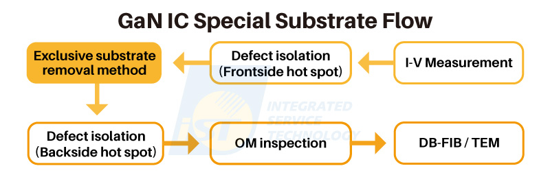
Figure 3: iST Failure Analysis Laboratory using unique solution to localize defects in GaN chips
(Source: iST)Step 1: Electrical Measurement Analysis and Defect Localization
When GaN chips experience electrical failures such as short, leakage, high resistance, or functional failures, they can be localized using various electrical failure analysis methods based on different failure modes. This involves applying direct current or powering up on a test board and utilizing suitable hot spot failure analysis tools. These tools may include Optical Beam Induced Resistance Change (OBIRCH), Thermal EMMI, and InGaAs, as listed in Table 1. By employing defect localization equipment, potential abnormal hot spots can be identified, facilitating subsequent Physical Failure Analysis (PFA). (Read more: Where to seek help for CIS chip defects?)
Equipment OBIRCH Thermal EMMI InGaAs Detection Targets Transistors/Metal Layers Metal Layers/Packaging/Printed Circuit Boards Transistors/Metal Layers Failure Modes Leakage, Short, High Resistance Leakage, Short, High Resistance Leakage, Short, Function Failure Table 1: Timing and use of various electrical measurement analysis equipment
(Source: iST)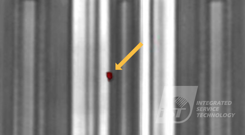
Figure 4: OBIRCH analysis image, hot spot can be observed at the top.
(Source: iST)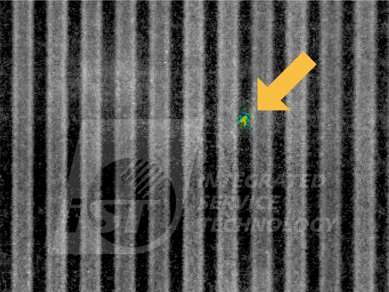
Figure 5: Thermal EMMI analysis image, hot spot can be observed at the top.
(Source: iST)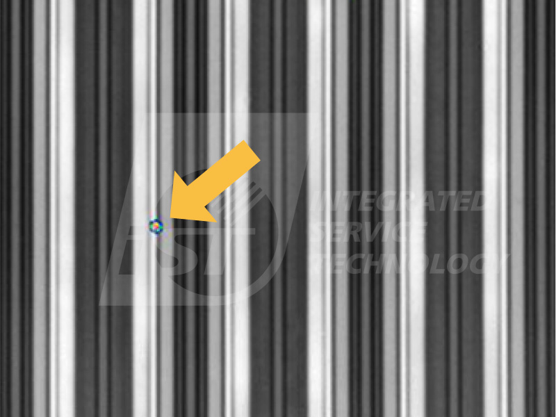
Figure6: InGaAs analysis image, hot spot can be observed at the top.
(Source: iST)Step 2: iST’s Exclusive Technique for Substrate Removal and Accurate Defect Localization
Traditionally, low-doped silicon substrates were commonly used, allowing for penetration with an infrared microscope and enabling standard backside analysis. However, as technology advances, there have been developments in substrate materials, including heavily doped silicon substrates and ceramics like AlN substrates (such as the QST substrate developed by GaN-on-Si substrate manufacturer Qromis). These new substrates are not easily penetrated by an infrared microscope, posing challenges for backside hot spot localization analysis.
To address this issue, iST has exclusively developed a novel substrate removal technique. This technique involves the optimized removal of various types of substrates, ensuring precise and uniform substrate removal while successfully achieving high-precision defect localization.
Step 3: Directly Observe the Hot Spots in the Defect Area with an Optical Microscope
Once an accurate positioning is achieved on the chip, the area that needs to be examined can be significantly reduced. Subsequently, a high-resolution optical microscope is employed for inspection. At this stage, it is often possible to identify defect, as illustrated in Figure 7, enabling successful localization.

Figure 7: Direct observation of defects using a high-resolution optical microscope in the hotspot area.
(Source: iST)Step 4: Backside DB-FIB or TEM Cross-sectional Analysis for Successful Defect Localization
Whether a potential defect is identified under an optical microscope or accurate hot spot localization has been achieved, the next step involves backside Dual-beam FIB (DB-FIB) and Transmission Electron Microscopy (TEM) cross-sectional analysis to confirm the defect’s structure and further clarify the root cause of the failure (as shown in Figure 8).
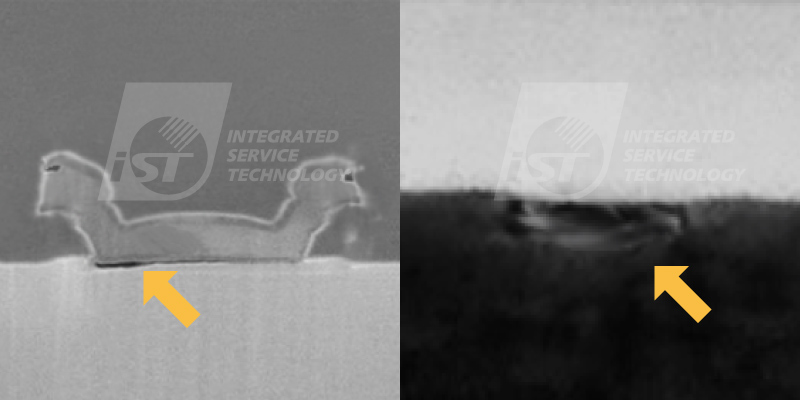
Figure 8: DB-FIB cross-sectional analysis (left image) and TEM analysis (right image) revealing abnormal details in the structure.
(Source: iST)Additional Note: After Step 1, Nano-Prober can also be Used for Precise Front Side Positioning, Followed by DB-FIB or TEM Cross-sectional Analysis.
In addition to iST’s exclusive backside analysis, Nano-Prober can also be employed for front side defect localization in certain special cases. This includes positioning methods such as Electron Beam Induced Current (EBIC), Electron Beam Absorbed Current (EBAC), and Electron Beam Induced Resistance Change (EBIRCH)(Figure 9)(Read more: Methods of precise positioning for defect detection based on nanoscale electrical characteristics measurement). Nano-Prober can also perform electrical measurements on transistors to obtain basic parameters like Vt, IdVg, IdVd, etc.
Once the defect is accurately localized using the above analysis techniques, the structure and elements can be further confirmed using DB-FIB or TEM.
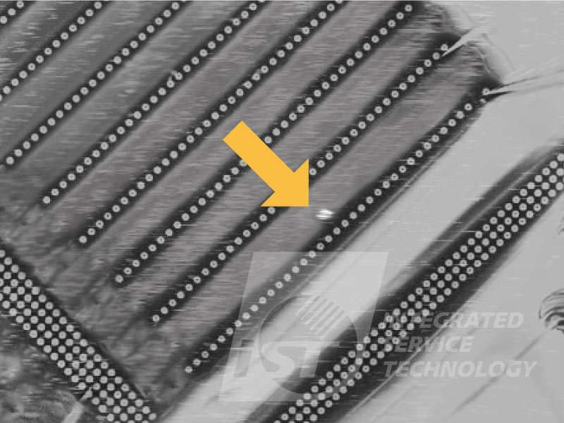
Figure 9: EBIRCH defect location analysis to more accurately localize defects for subsequent execution of DB-FIB or TEM.
(Source: iST)
iST ‘s exclusive substrate removal technology has allowed for the backside localization of hotspots in samples, solving the challenges in GaN chip failure analysis. Combined with electrical measurements and physical failure analysis, this one-stop analysis approach has successfully improved the defect localization rate. This breakthrough is contributing to the rapid development of GaN in multiple application areas, bringing high-performance and reliable semiconductor components.
This article is shared with all of you, our long-standing supporters of iST. If you would like to explore further details, please feel free to contact
Kuolin Cheng at +886-3-579-9909 Ext 6758 or via email at IST_FA_IAD@istgroup.com or marketing_tw@istgroup.com.