Issued Date:2021/9/28SEM BSE
Issued By:iST
What should you do when SEM cannot distinguish substances of samples by layers?
No defects found with SEM even the defected ICs have been delayered?
You may have encountered both cases in your daily work. You may be baffled by sample IC with hot spots determined by electric measurement yet not one layer of it can be blamed for the defects due to limited features of general Scanning Electron Microscope (SEM) including poor resolution and contrast of substances.
We at iST are well informed about your needs to tackle this issue! The Backscattered Electron (BSE) is the tool you can rely on. The SEM images with Secondary Electron (SE) and Backscattered Electron (BSE) excited by electronic beams. Differing from conventional SEM device, with SE imaging by secondary electron detector, the YAG BSE Detector implemented by iST last year helps you to pinpoint hot spots with BSE images. With more than 400 successful cases since then, this iST Classroom is here to show you the three features of SEM BSE.
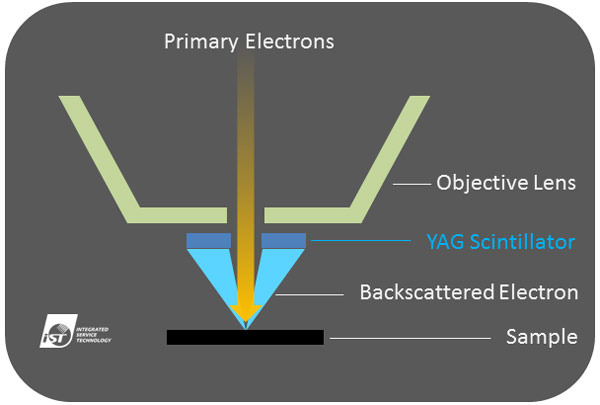
SEM BSE
Featuring Yttrium Aluminum Garnet, the YAG BSE Detector is located between the electromagnetic lens and samples, and receives backscattered electrons signals for imaging.
1. Better contrast between different substances
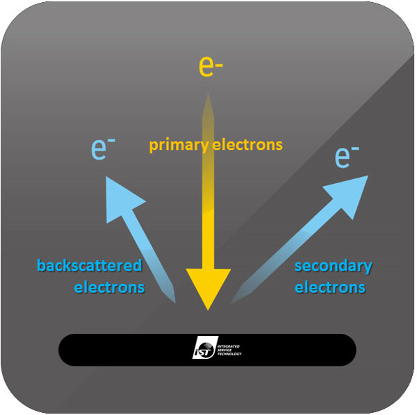
Figure 2: Backscattered electrons are those bounced back by electron beams when hitting the atomic nucleus.
Backscattered electrons are those bounced back by electron beams when hitting the atomic nucleus on a sample surface. Elements of larger atomic numbers would backscatter more electrons. That is, the brighter area on SEM image is very likely where substances of larger atomic numbers are located.
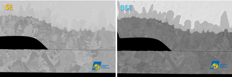
Figure 3: SE image on the left hand side and the BSE on the right suggest that the BSE renders a better contrast of brightness for the Sn-IMC-Cu substance.
2. Suitable for observing the defects of bottom layers of ICs
Electrons backscattered by electron beams hitting the atomic nucleus hardly suffer energy loss. That is, they come with much more energies than that of the secondary electrons, in turn; give the backscattered electrons more energy to escape from the sample into the BSE detector. Comparing the images of secondary electrons, the backscattered ones reflect the status of the deeper layers.
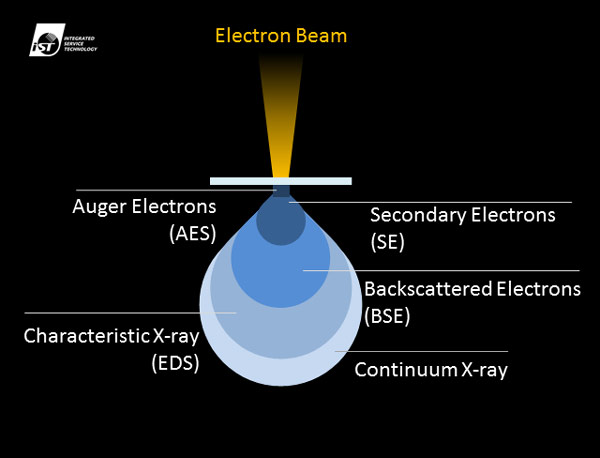
Figure 4. Signals of backscattered electrons come from the deeper layer of samples.
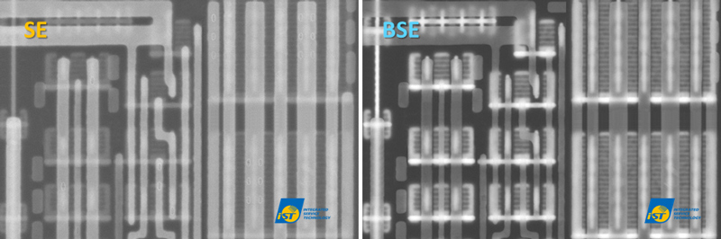
Figure 5. BSE image is suitable for observing the lower layer of FinFET structure, and can avoid the risk of over polishing.
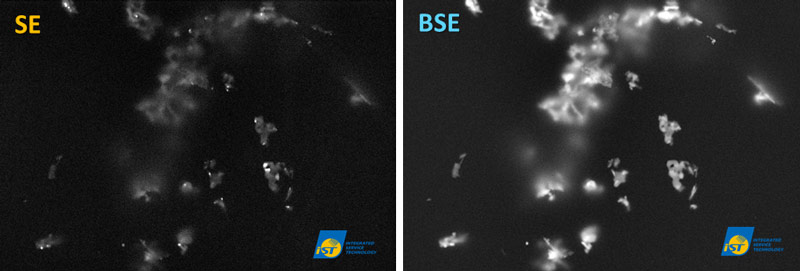
Figure 6: Thanks to easily penetrating the liquid platform’s silicon nitride film and good contrast of substances, the BSE is ideal for observing images of particles of grinding solutions. (Read more: How to Detect Liquid Material Defects with SEM?)
3. Less charging effect. Samples with poor conductivity can also be imaged smoothly
Differing from secondary electrons’ shallow layer signals and tending to accumulate charges on the surface of samples, the backscattered electrons’ poorer surface charge accumulation enables it to image samples with poor conductivity or without conduction coating.
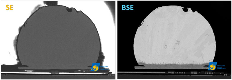
Figure 7: Image of samples with poor conductivity by the BSE detector.
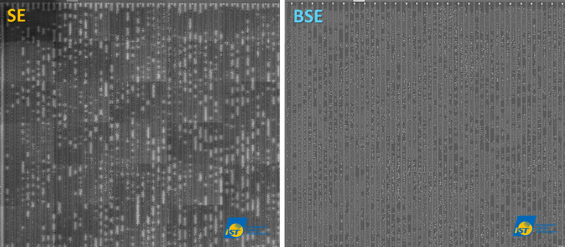
Figure 8: SE images tend to accumulate charges and result in poor brightness uniformity of and mosaics on the figures of images stitched together. This is not the case with the BSE images. (Read more: How to use SEM full-vision imaging technology to reverse-perceive nano-scale processing while avoid infringement?
This article is aimed to share our experiences with honorable clients like you. In case you want to know more details, please call Mr. Chen at +886-3-579-9909 Ext. 6641 or email: web_pfa@istgroup.com
Other services you may be interested in
SEM BSE