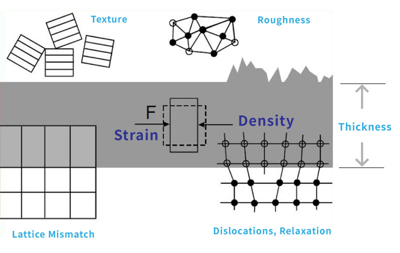
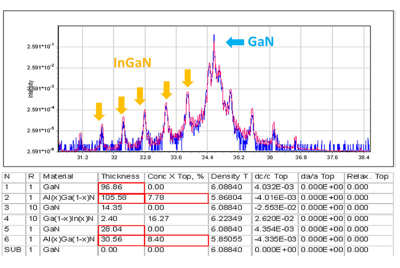
X-ray diffraction analysis (XRD), is designed to identify material crystal structure, crystal orientation, and grains size of nanometer crystal, as well as residual stress analysis of mono- and poly-crystalline film material by pairing the X-ray diffraction pattern of crystal against databases in a non-destructive manner.
The Superiority of iST
Case Sharing
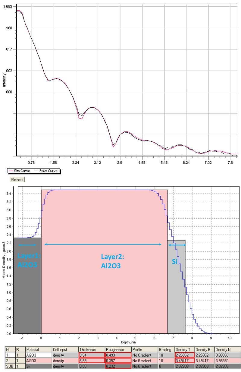
Sample for analysis: Al2O3/Si
See figure below for results of fitting the XRR pattern of aluminum oxide films on silicon substrate. The table below suggests there are two layers of aluminum oxide films at different densities (the thickness is 0.94 nm and 6.69 nm for upper and lower layer respectively); roughness of aluminum oxide surface and the silicon substrate interface is 0.49 nm and 0.23 nm odd respectively.
- Crystal structure analysis (lattice)
- Crystallinity analysis
- Texture analysis
- Thin film residual stress analysis
- RSM (Reciprocal Space Mapping) analysis
- XRR analysis
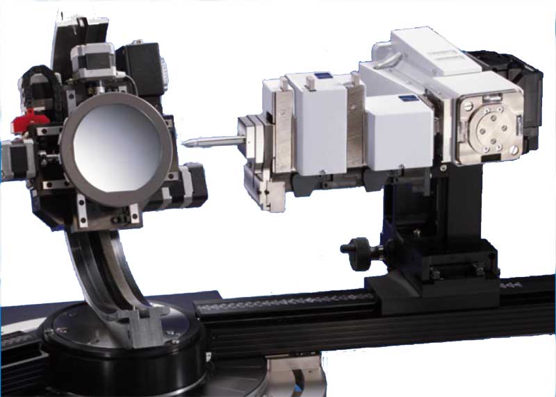
Bruker New D8 Discover
| X-ray source | 6kW turbo X-ray spot size: 0.3*3mm |
| Detector | LynxEye PathFinder |
| Other functions | 2 bounce monochromator Ge (002) Laser alignment |
- Semiconductor Industry
- LED Industry
- Optoelectronics Industry
- Nanomaterials R&D
Contact Window | Mr. Chiang/Neal | Tel:+886-3-5799909#6176 | Email: web_ma@istgroup.com

