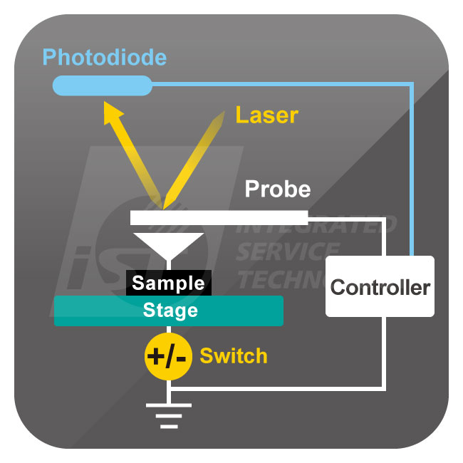
C-AFM and AFM share similar principles, both relying on the force between the probe tip and the surface atoms of the sample to reveal the surface morphology. The difference lies in the fact that, during the scanning of the sample, C-AFM has the capability to simultaneously apply bias voltage and extract current through the conductive probe, resulting in a current map. Through interpretation, electrical anomalies on the sample can be identified.
What iST can do for you?
The general failure analysis method typically involves first electrical fault isolation (hotspot detection) and then using a Scanning Electron Microscope (SEM) to observe layer by layer for defect identification. However, because SEM lacks quantitative electrical measurement capabilities, certain defects may be missed by SEM voltage contrast (VC) analysis. In such cases, C-AFM is able to scan a wide range of the target area to extract current, by applying bias from the sample backside with a conductive probe. Hence, the electrical characteristics of the abnormal location is easily to be revealed, whether the leakage or open failures caused of defect occurred at the P-junction, the N-junction, or the bulk.

The Superiority of iST
iST’s one-stop failure analysis solution can help you detect hot spots through electrical failure analysis, perform SEM and C-AFM analysis after Decap/Delayer, and further use Nano-Probe electrical measurements to precisely localize the defects. Subsequent material analysis, such as dual-beam focused ion beam (DB-FIB) or transmission electron microscopy (TEM) analysis, can be conducted to identify the root cause of the defects.
Case Sharing
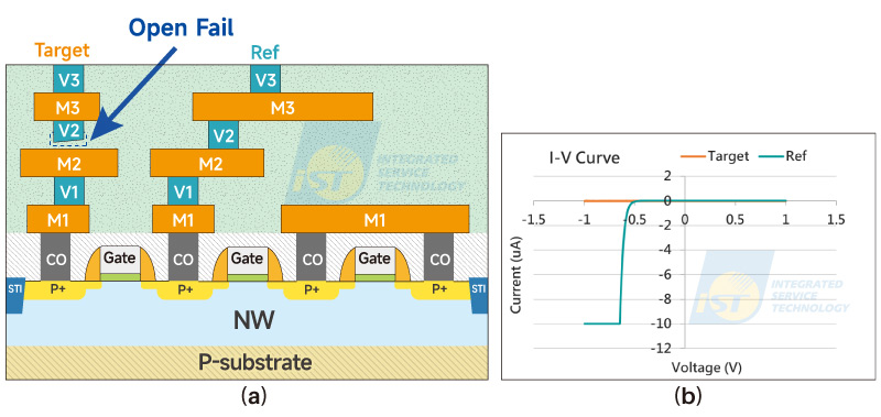
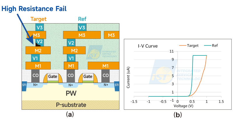
(a) Schematic diagram of process open circuit failure;
(b) I-V curve results from C-AFM.
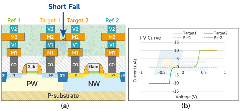
(a) Schematic diagram of process short circuit failure;
(b) I-V curve results from C-AFM.
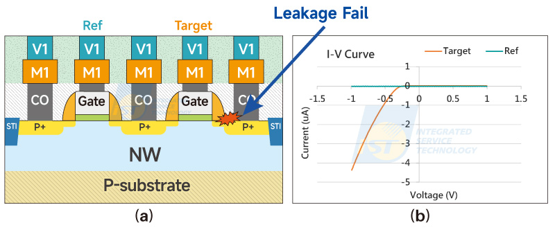
(a) Schematic diagram of process gate leakage failure;
(b) I-V curve results from C-AFM.
(a) Schematic diagram of process gate leakage failure;
(b) I-V curve results from C-AFM.
Max. voltage for sample I-V curve measurement: ±10 V; Max. current limit of 1 μA; a sample diameter requirement of less than 2 cm, and a maximum scanning range of 50x50 μm2。
Contact Window | Ms. Hsu/Yating | Tel: +886-3-5799909#6699 | Email: web_EFA@istgroup.com