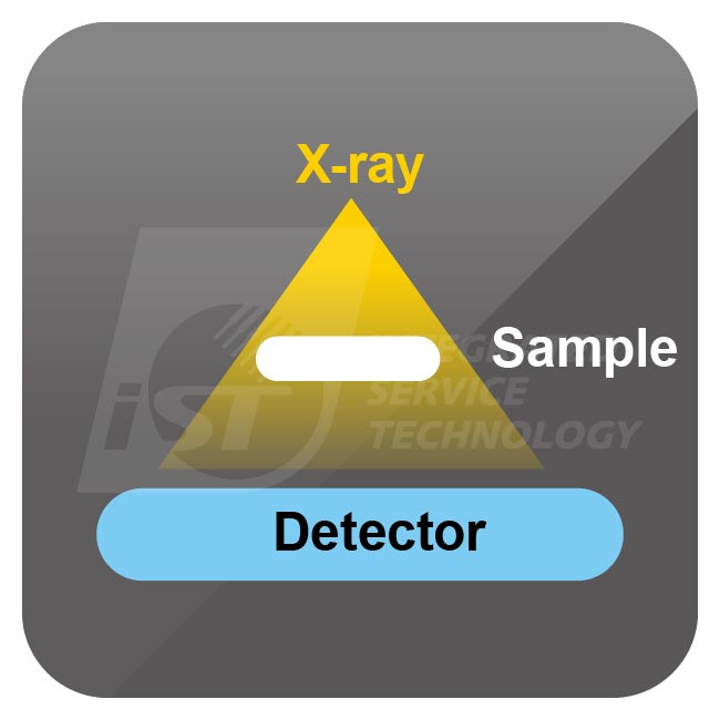
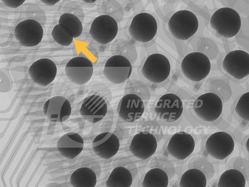
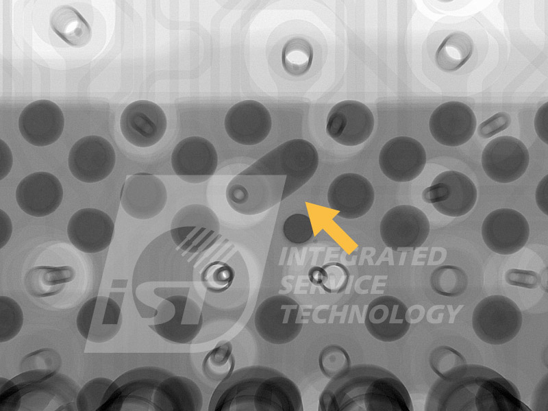
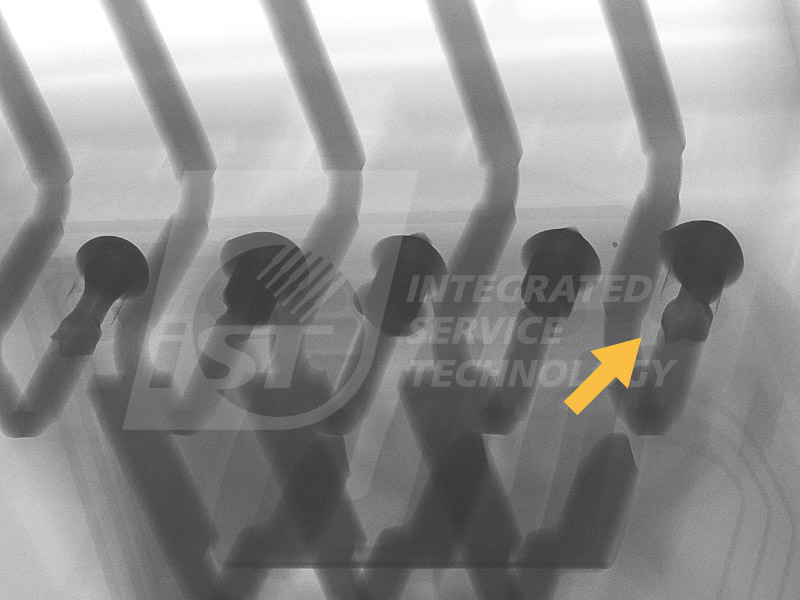
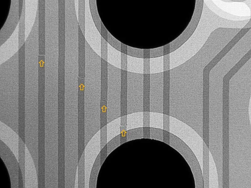
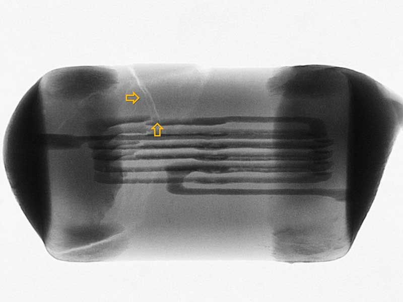
X-ray is very powerful in penetrating objects. The level of penetration varies with the density of the substance contained in an object structure. The X-ray receives images based on the amount of penetrated energy.
The Superiority of iST
Case Sharing
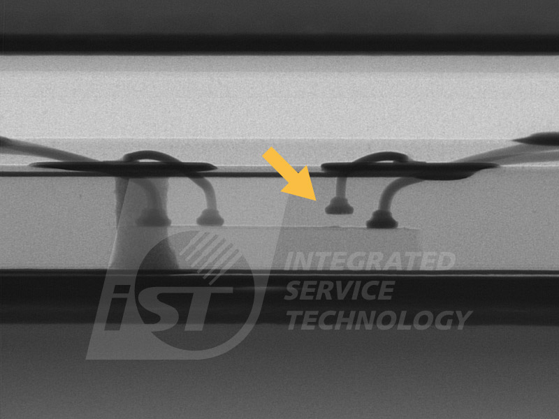
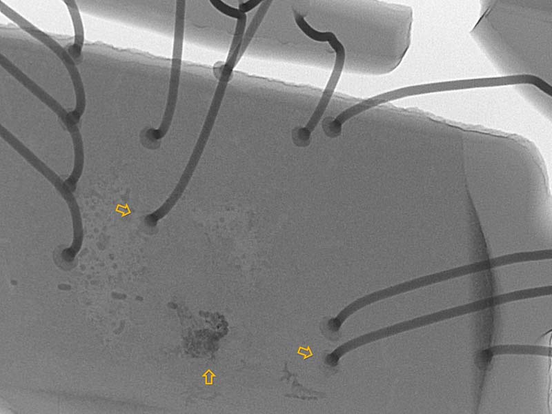
- Defect inspection in IC packaging: layer delamination, burst Crack, void, and bonding inspection.
- Potential defects in the PCB manufacturing process e.g.: misalignment, bridge or open circuit.
- SMT soldering void inspection and measurement.
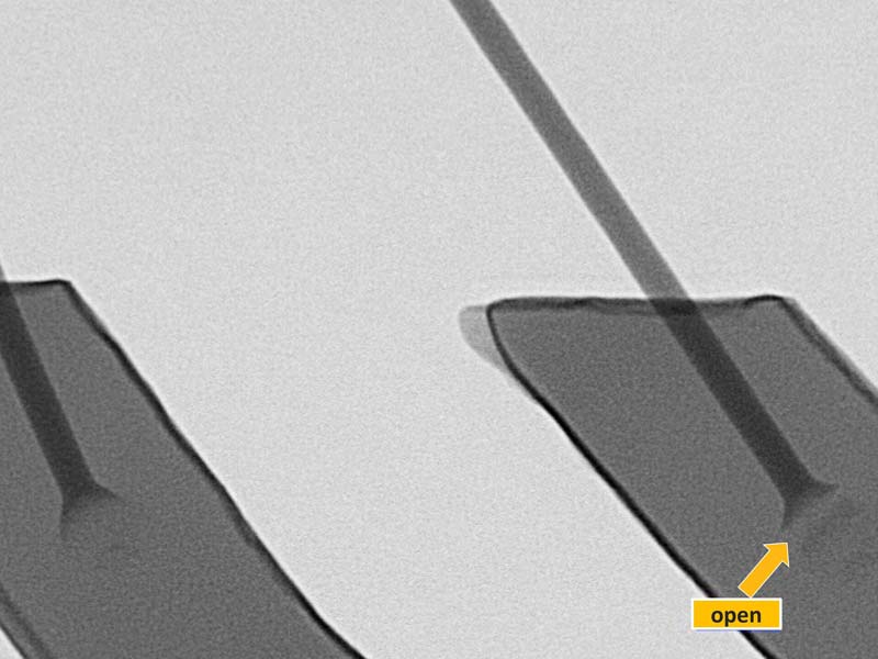
- Defect inspection of open, short or abnormal connections in the interconnect.
- Solder ball array inspection in BGA packaging and flip chip packaging.
- Inspection of crack in high density plastic material or void in metal.
- Chip dimension measurement, wire arc measurement, soldering percentage measurement.
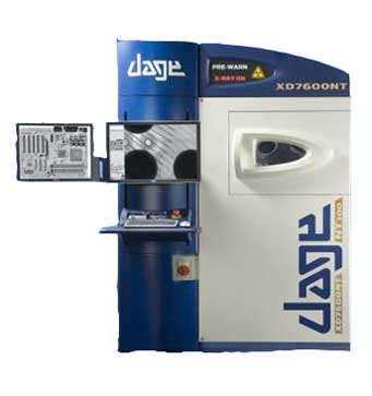
Dage XD7600 NT100 Diamond
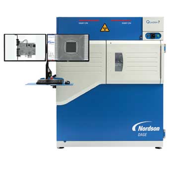
Dage Quadra 7
- Real time image
- Measurement image dimension
- Max magnification of 1920 (depending on sample size)
- X-ray Spot Size: 0.1μm
- Tilt angle 66゚, 360゚rotation
- Diamond 160kV, 10W; Quadra7 160kV, 20W
- Inspection area 45cm (L) x 40cm (W) x 10cm(H) / weight 5kg
Aluminum wires or low density materials used in IC packaging are not applicable to X-Ray inspection.
Contact Window | Mr. Chang/HP | Tel:+886-3-5799909#6580 | Email:web_nde@istgroup.com

