Issued Date:2024/9/5 SiPh
Issued By:iST
In 2020, Intel identified silicon photonics as a key technology for Advanced Packaging. Now, four years later, silicon photonics has truly become a critical focus of R&D in the semiconductor industry. It is expected that in two years, this technology will be fully integrated and operational. As we stand on the brink of this transformative shift from “electrical” to “optical,” are you ready for this revolution?
SiPh

As semiconductor integrated circuit technology continuously advances, we have witnessed the evolution of Moore’s Law. The miniaturization of component sizes and the application of new materials aim to increase the number of components per unit area, thereby accelerating IC processing speed, improving heat dissipation, and conserving energy. However, as miniaturization approaches physical limits, process technology faces challenges, and yield issues have emerged.
In response to this challenge, experts have begun exploring new approaches such as integrating different functional ICs into a single chip and adopting 3D stacking packaging technology. However, these technologies still fundamentally rely on metal wires to connect the various components. Since the inception of chips, “electrons” have been the primary medium for signal transmission, with their transmission speed directly determining chip performance. In recent years, the demand for high-performance computing (HPC), artificial intelligence (AI), and cloud data has grown explosively. How can we break through these limits to achieve more efficient transmission? Thus, attention has turned to “photons.” Could the introduction of faster “photons” accelerate the operation of components?
SiPh
SiPh
Optical fiber systems used in optical communication can transmit data around the world at speeds of trillions of bits per second, an idea envisioned by Bell Labs engineers as early as 1968. By the early 21st century, it was discovered that photonic technology could facilitate data transmission not only between countries but also within data centers, between CPUs, and even between chips. The reason for adopting “light” is that glass (SiO2) is transparent to light and does not cause interference. Essentially, data can be transmitted at high speeds through optical waveguides within SiO2, which are capable of transmitting electromagnetic waves.
Silicon (Si) has a refractive index of 3.5 at infrared wavelengths, which means it can bend or slow down light more effectively than many other materials used in optics. The typical wavelengths for optical transmission are 1.3 and 1.55 micrometers, and silicon does not absorb light at these wavelengths, allowing light to pass directly through it. This compatibility enables silicon-based devices to transmit large amounts of data over long distances without significant signal loss.
Therefore, silicon photonics technology leverages the mature CMOS silicon (Si) technology combined with photonic device processing, enabling data transmission speeds between processor cores to increase by hundreds of times while consuming less energy. In addition to the ever-growing demand for high-performance computing and artificial intelligence, photonic devices are also highly suitable for applications like optical radar and biomedical sensing. Major IC manufacturers worldwide have successively declared that silicon photonics is the key and trend for future IC technology. In this issue, the iST classroom shares relevant literature to help you understand the composition of silicon photonic devices and the key factors determining their performance. SiPh
1. Composition of Silicon Photonic Devices: Germanium as the Material of Choice
The basic components of silicon photonic devices include a p-i-n diode (PIN diode) photodetector that converts light into electrical signals, an optical waveguide for signal transmission, and modulators and couplers that convert electrical signals into photons. These elements are combined into a single chip, with the cross-sectional structure generally shown in Figure 1.
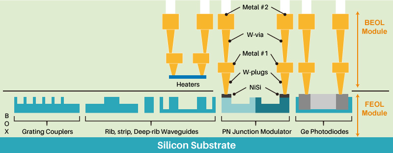
Figure 1 : Cross-sectional schematics of the full CEA LETI’s silicon photonic platform
for monolithic integration of passive and active chip components. [1]
(Image source:D. Benedikovic et al., Nano-Photonics, 2021, 10(3): 1059–1079)The most critical manufacturing technology is found in the PIN diode on the right side of Figure 1. Germanium (Ge) is the preferred semiconductor material due to its quasi-direct band gap and a small band gap of 0.8 eV, which is lower than the photon energy. Additionally, germanium’s high absorption coefficient for light makes it ideal for photodetectors and an excellent alternative material. SiPh
A PIN diode is composed of a highly doped P (p+) type region and a highly doped N (n+) type region, with an intrinsic (I) layer sandwiched between them. Under reverse bias, the depletion width (Wd) of the diode extends across the entire intrinsic layer. As illustrated in the band structure of Figure 2, when photons are absorbed in the intrinsic layer, electron-hole pairs are generated between the conduction and valence bands, which then drift to form a current. The primary focus in the development of silicon photonic devices is to optimize the performance and bandwidth of the PIN photodetector process while maintaining the characteristics of conventional CMOS devices.
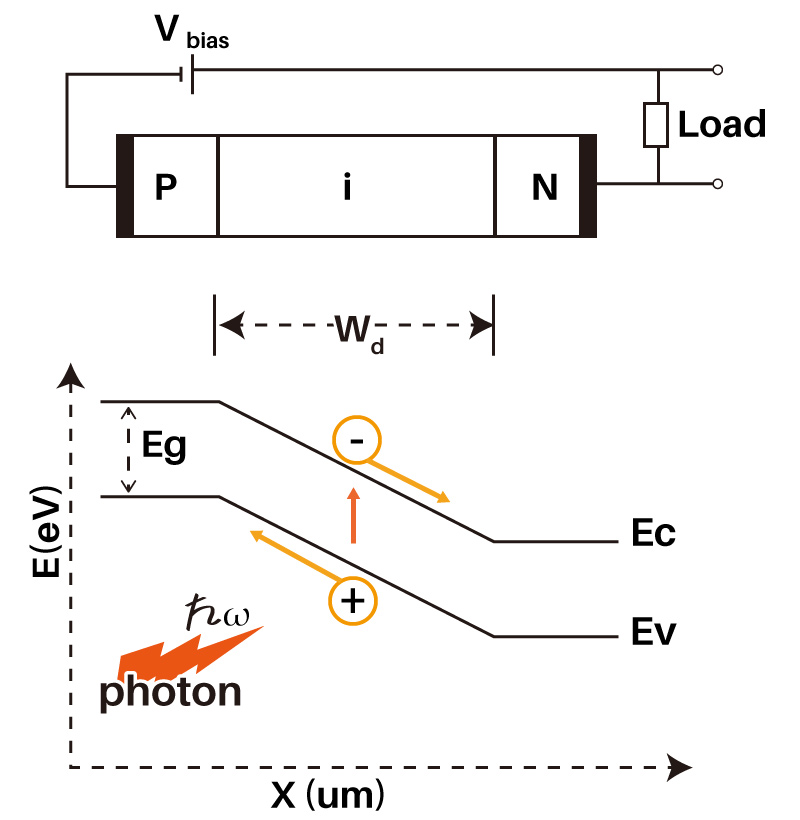
Figure 2: P-i-N photodetector showing the doping structure and the energy band diagram of the diode under reverse bias.[2]
(Image source: J. Nxumalo et al., IEEE, 2018)
2. How to Identify the Quality of a Ge-PIN?
First, let’s use Figure 3 to briefly explain the design of a single chip, showing the relative positions of the Ge-PIN photodetector and the Si-waveguide. Figure 3(a) is a schematic of the cross-sectional structure, with the waveguide located below the intrinsic layer, while Figure 3(b) is the top layout.
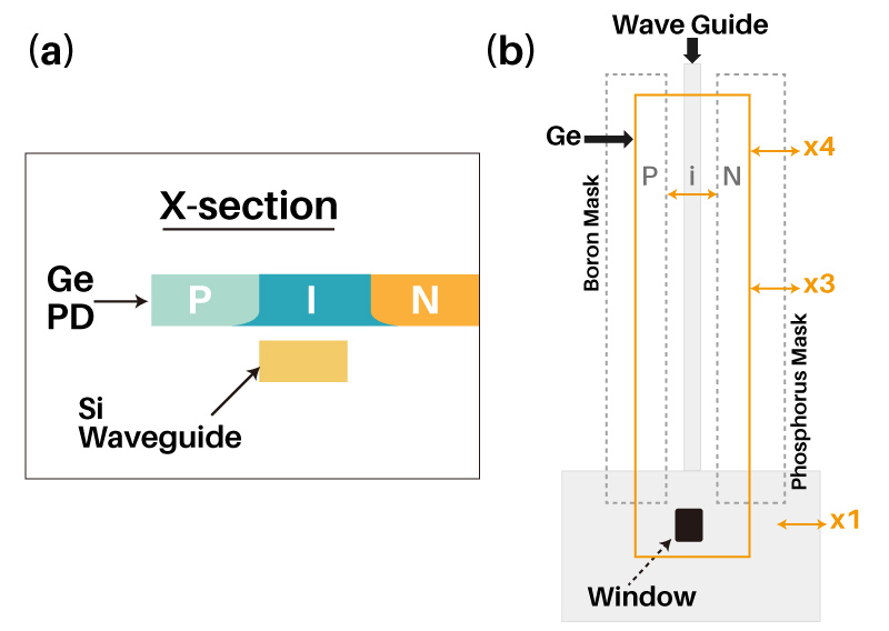
Figure3 : (a)cross-section illustration of doping structure, and (b) photodetector layout showing analysis cross sections [3]
(Image source: J. Nxumalo et al., IEEE, 2018)
The quality of Ge-PIN diodes significantly affects the optoelectronic performance of the detectors. The epitaxial process of Ge on Si can lead to lattice mismatch and dislocation defects caused by ion implantation, impacting quality. Figure 4 shows the Ge-PIN observed through a Transmission Electron Microscope (TEM). It is evident that both the intrinsic layer and the P region appear bright, indicating no significant defects. In contrast, the N region on the right side appears dark gray, likely due to lattice defects resulting from the ion implantation process. (Further reading: Decode Semiconductor Dislocation Traces Unveil Chip Leakage Causes with TEM)
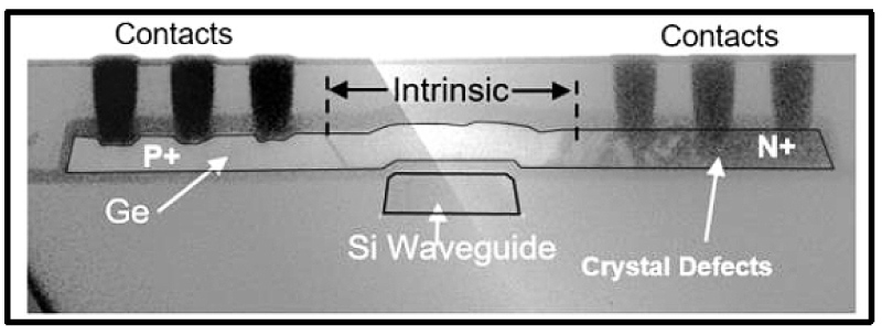
Figure 4 :TEM cross-section of a Ge photodetector. [4]
(Image source: J. Nxumalo et al., IEEE, 2018)Additionally, EDS analysis can be used to determine whether Si in the waveguide has diffused towards the Ge-PIN. Figure 5 shows the Si content distribution along the waveguide direction in the Ge layer. The Si mole percentage decreases from about 35% at the contact window to below the EDS detection limit of 2% at approximately 11 mm from the input side, indicating significant diffusion.
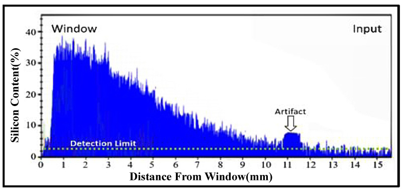
Figure 5: EDX spectrum shows Si distribution from the window (0mm) to the input (15mm) of photodetector. [5]
(Image source: J. Nxumalo et al., IEEE, 2018)3. How to Observe the Depletion Width Affecting Photodetector Performance?
The primary process for silicon photonic devices is CMOS. By using Scanning Capacitance Microscopy (SCM) analysis, the depletion width (Wd) in the intrinsic layer can be measured under different process conditions. Figure 6 illustrates how the 2D carrier mapping image and the 1D carrier line profile obtained from SCM can be used to identify the P/N junction position and visualize the Wd.
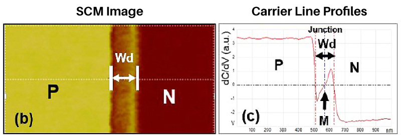
Figure 6 : SCM cross-section of the PIN, showing 2D carrier mapping image and 1D line profile. [6]
(Image source: J. Nxumalo et al., IEEE, 2018)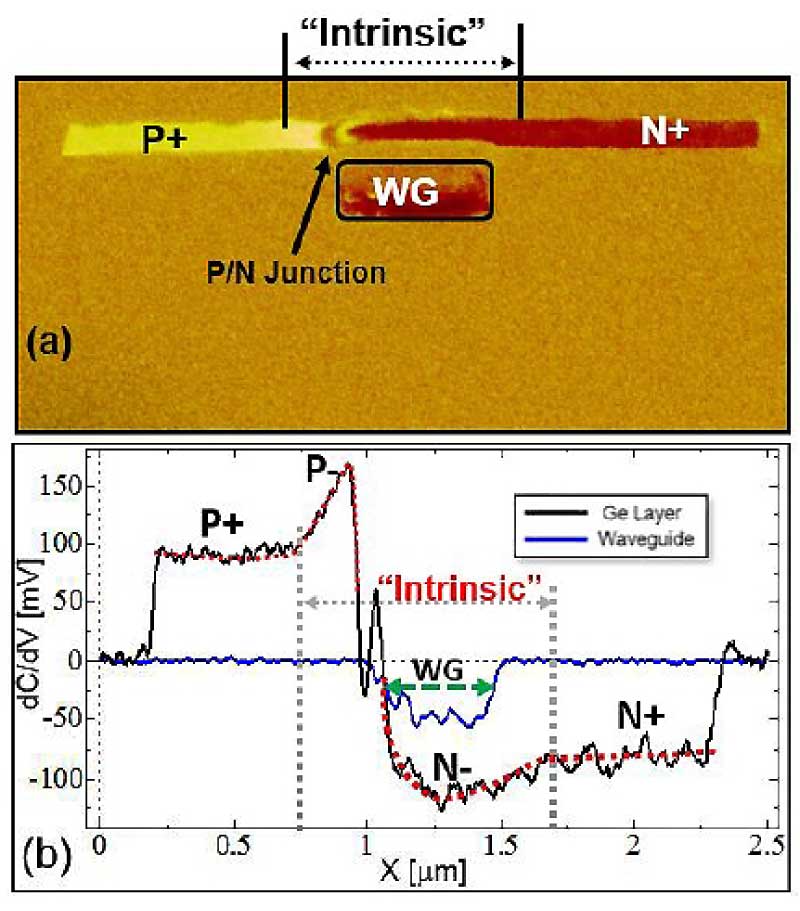
Figure 7: SCM image at the X3 position in Fig. 3(B), showing(a) 2D carrier map and (b) lateral 1D carrier profile. [7]
(Image source: J. Nxumalo et al., IEEE, 2018)In Figure 3, the one-dimensional carrier distribution results of the cross-sectional SCM at the X3 and X4 regions are shown in Figure 8. It can be measured that the p/n junction position has shifted by approximately 215 nm (the distance between the two dashed lines). The changes in the depletion width (Wd) can be observed through SCM, and the depletion width determines the amount of current that flows, which directly impacts the quality and performance of the device.
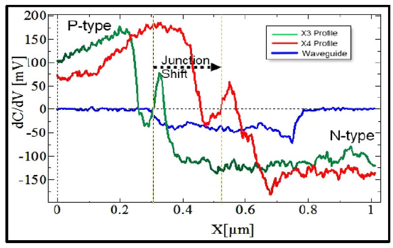
Figure 8 : Line carrier profiles showing p/n junction displacement between X3 and X4 planes in Ge photodetector. [8]
(Image source: J. Nxumalo et al., IEEE, 2018)This article discusses factors such as lattice defects caused by ion implantation, the diffusion of silicon waveguides towards the intrinsic layer, and the different diffusion rates of N/P dopants that affect the depletion width (Wd). These elements all determine the quality of silicon photonic devices and are the current challenges faced in the R&D of single-chip silicon photonics process technology.
SiPh
Additionally, in the design of waveguide materials or shapes and other related process developments, nano-material analysis techniques such as TEM, EDS, and SCM can be utilized. iST has extensive practical experience in material analysis and can provide customers with effective concentration distribution data analysis, which can be used to improve the details of R&D processes.
In fact, most existing silicon photonics products integrate digital switching chips and optical transceiver modules using advanced packaging techniques, commercialized as Co-Packaged Optics (CPO). These products still face issues with energy consumption and bulkiness. In the future, adopting “single-chip silicon photonics” can truly achieve the goals of compactness and energy efficiency. This technology can provide high-speed, energy-efficient integrated solutions, fundamentally transforming industries such as data centers, artificial intelligence, telecommunications, sensing and imaging, and biomedical applications.
The iST Materials Analysis Laboratory has long observed trends in the semiconductor industry. We believe that despite the challenges related to integration and device manufacturing in silicon photonics technology, major manufacturers will continue to accelerate their R&D efforts. With global collaboration, the breakthrough in key technologies that surpass Moore’s Law is imminent. SiPh
We appreciate the ongoing support from you all. If you would like to further understand the details, please feel free to contact Mr. Chang at +886-3-579-9909 ext. 6613 or via email at sa_tw@istgroup.com;marketing_tw@istgroup.com.
Reference:
[1] Daniel Benedikovic*, Léopold Virot, Guy Aubin, Jean-Michel Hartmann, Farah Amar, Xavier Le Roux, Carlos Alonso-Ramos, Éric Cassan, Delphine Marris-Morini, Jean-Marc Fédéli, Frédéric Boeuf, Bertrand Szelag and Laurent Vivien, “Silicon–germanium receivers for short-wave-infrared optoelectronics and communications”, Nano-photonics 2021; 10(3): 1059–1079
[2] -[8] J. Nxumalo, Y. Wang, M. Iwatake, C. Molella, A. Katnani, J. Orcutt, J. Ayala, K. Nummy, “Characterizing junction profiles in Ge photodetectors using scanning capacitance microscopy (SCM) and electron holography”, 978-1-5386-4513-0/18 ©2018 IEEE