What is a Probe Card and When is it Used?
A probe card is a critical interface tool used during the wafer test (Wafer Sort Test /Chip Probing) stage of semiconductor production. Before the ICs are diced and packaged, precise electrical testing is performed to ensure they meet mass production quality. By using a probe card, each die on the wafer can be accurately connected to the automated test equipment (ATE) for electrical verification. This process effectively screens out defective chips early, stabilizes and streamlines the testing workflow, and ultimately improves packaging efficiency and overall production yield.
Advantages of iST Probe Card Design
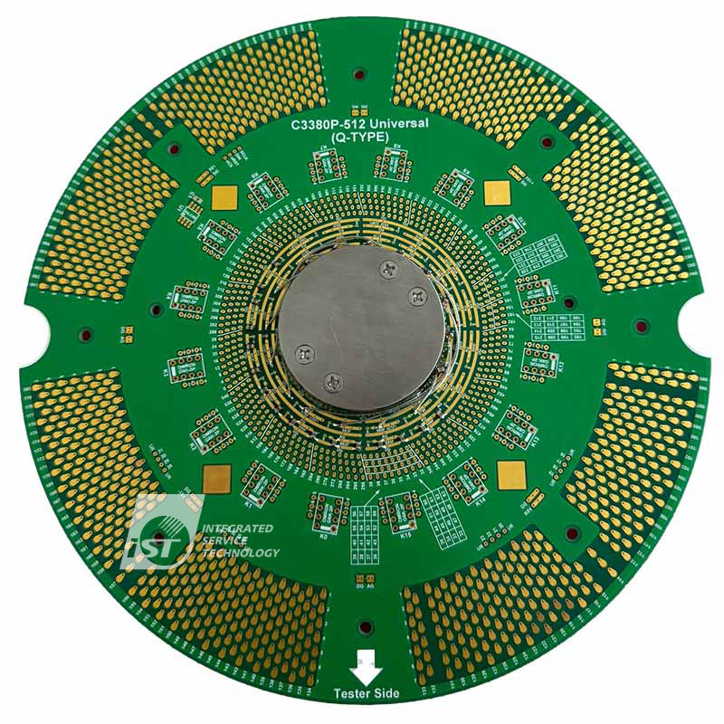
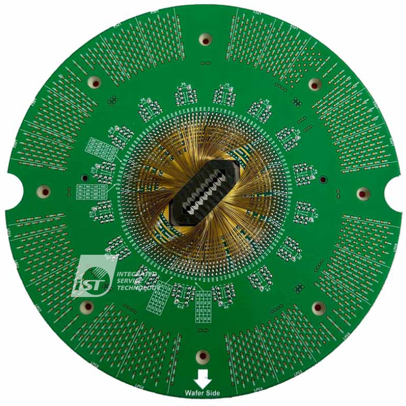
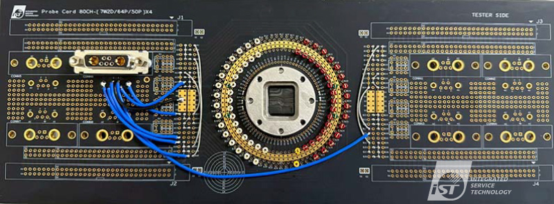
Types of iST Probe Cards
- Advantest: EXA, V93K, T2000, ND1~4
- Teradyne: Ultraflex+, Ultraflex, J750, ETS
- Cohu: Diamondx, D10, ASL
- NI: STS
- Chroma: 3360, 3350, 3380, 3680
- KYEC: E320, I6000, I2K
- YTEC: S50, S100, S300 For other inquiries, please contact us.
- IC Design Companies: Verification of new projects, high-frequency testing for AI and HPC applications
- Foundries (Wafer Manufacturers): Verification of WAT and E-test process parameters
- OSAT (Outsourced Semiconductor Assembly and Test) Companies: Support wafer testing for mass production, optimize contact reliability and durability
- IDM Companies: Support verification across various internal package types and high-reliability conditions
- Automotive / High-Performance IC Manufacturers: Support high-power, high-temperature, and 3D packaging applications
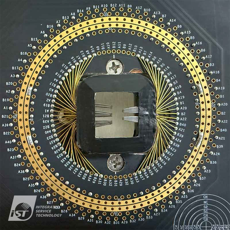
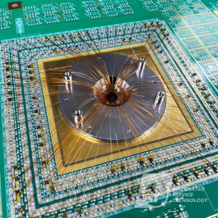
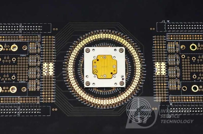
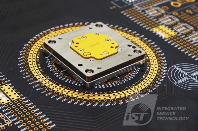
A high-performance, stable probe card relies on the careful design of the following five key components. iST ensures their performance and longevity through rigorous verification processes:
| Component | Design Focus | iST Approach |
|---|---|---|
| Needle | Geometry and material directly affect contact stability and mark control | Select optimal probe type based on DUT characteristics, e.g., cantilever or vertical, alloy or low-resistance, pointed or flat-tip |
| PCB | Signal transmission stability, crosstalk suppression | High-speed routing design with SI/PI simulation verification |
| Interposer | Pitch conversion and structural support | Custom WST, MLC, MLO interposer layers to accommodate various package types |
| Active Components | Optimize signal and power integrity | Embed R/C components and optimize matching through simulation and measurement |
| Stiffener | Vibration damping and overall alignment precision | Use low thermal expansion materials to enhance test stability |
Contact Window | Ms. Lin/Aaliyah | Tel:+886-3-5799909#8890 | Email:HWBU_Sales@istgroup.com