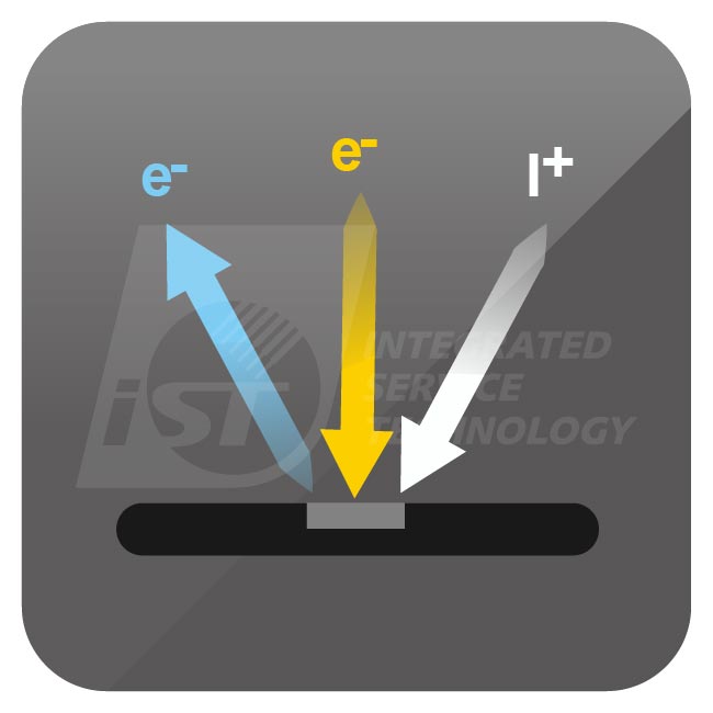
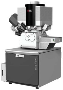
The principle of Plasma FIB (P FIB) is similar to Dual Beam FIB (DB FIB), the difference is as follows:
| Ion source | Xe+ Ion plasma | Ga+ Ion |
|---|---|---|
| (Probe current) | 1.5 pA~2.5 μA | 1.1 pA~65 nA |
- Ga Ions used by DB FIB tend to attach to the sample surface; instead, Xe used by P FIB reduces sample contamination by Ga Ions.
- P FIB is capable of running over large areas more than 20 times faster than DB FIB.
Case Sharing
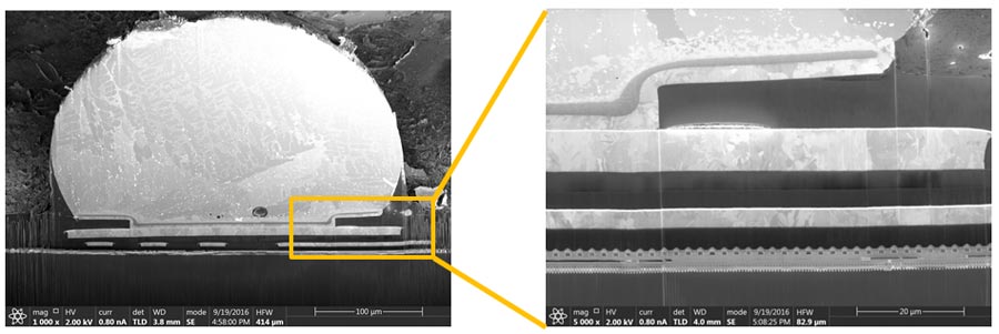
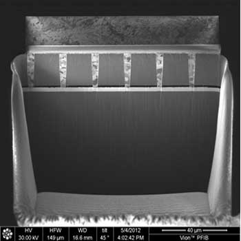
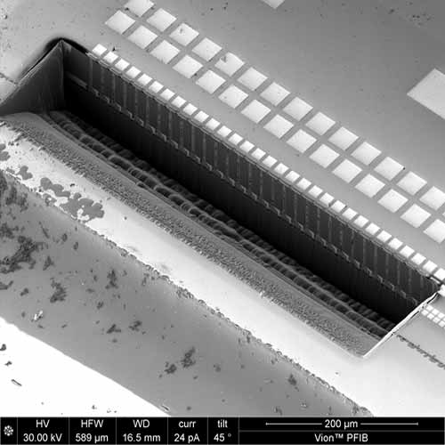
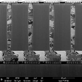
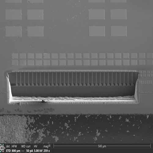
- Large range structural observation (100μm or more) including 3D, TSV, solder ball, Cu pillar, and packaging products (WLCSP FA), etc.
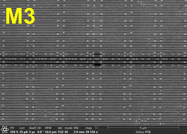
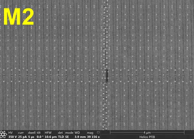
- Delayer application for advanced processing of 28nm or narrower.
Contact Window | Dr. Lin/Weijui | Tel:+886-3-5799909#6166 | Email:web_ma@istgroup.com

