Issued Date:2021/9/14surface analysis
Issued By:iST
Which tool can be used to identify the contamination which led to the failure now?
Which contamination requires a surface analysis tool?
Which surface analysis tool should be chosen to catch process defects?
Hardly any semiconductor process can be spared of some contamination. Common foreign particles are easy to identify with the help of optical or electron microscope but not residuals left by surface oxidation and micro-etching. The latter usually come at layers with thickness of just several atoms, i.e., nanometers, and with chemical characteristics that differ from the solid materials which, in turn, enable them to escape the lens of general microscope. Yet they make terrible errors later including coating delamination, package wire bonding, reball failure, over-raised resistance or poor electrical property. Identifying these foreign matters invisible to the human eyes or microscope mandates the help of surface analysis tools.
This iST Classroom will share with you “how to use surface analysis tools to catch defects in the semiconductor process.”
surface analysis
Very tiny and thin or even nano-scale foreign matters may have been left since the very beginning of semiconductor manufacturing and thus it is hard to determine which process should be blamed. They may be residuals left by oxidation or contamination in the RDL or UBM process and result in poor electrical property, high resistance (or open circuit), short circuit, or electric leakage. These invisible defects mandate surface analysis tools to catch them.
I. When to Use One of the Five Surface Analysis Tools?
■ Profile and dimension bumpy surface – SEM
The scanning electron microscope (SEM), a relatively well-known materials analysis instrument, is used to profile and dimension a bumpy surface. SEM can image a surface based on secondary electronic signals caught by scanning the sample’s surface or work with X-ray energy dispersive spectroscopy (EDS) to identify its elements.
■ Identify oxidized, corroded or contaminated nano-thick film – AES/XPS
The problem with SEM is that it’s hard for it to detect several nano-thickness contamination (a layer of couple of atoms stacked together) on the top surface as the data it collected came from X-ray signals echoed by substance hundreds of nanos deep down.
Here comes the Auger Electron Spectroscopy (AES) and X-ray Photoelectron Spectroscopy (XPS). These two are used to identify oxidation, corrosion and contamination in most cases. In such cases they may work with the argon ion sputtering based depth profile analysis technique to determine the thickness of the oxidation or corrosion layer.
See Figure 1 for the outcome of a typical Al pad surface’s qualitative analysis by AES. The energy spectrum on the left suggests that residuals left on the surface are elements C, O, F and Al while the right one, the outcome of depth profile analysis, suggests the depth dependent distribution of individual elements. The latter can be used to estimate thickness of the oxidation layer and contamination by F-element on the surface (24nm and 13nm, respectively). The oxidation corrosion residuals are the result of over storage or the F-contamination of the CF4 gas for dry etching in the opening process of Al pad. Both are key factors in determining the wire bonding quality later when packaging.
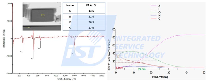
Figure 1: Residual elements on IC Al pad surface by AES and depth profile analysis for oxidation layer thickness.
Regarding analysis over residuals on the post-process side wall of TSV Vias by advanced 3D packaging and surface oxidation in the copper pillar process: the micro-electronic beam of the AES can be used to analyze surface residuals on the Via inner wall or bump of the diameter up to tens of microns.
However, AES cannot work with insulating samples as the triggering electronics would charge the surface of non-conductive materials and impair capturing AES signals. This is not only its most critical disadvantage but also makes it differ from SEM as we can coat the sample with a metal layer for SEM measurement and observation.
■ Test non-conductive samples with a surface greater than ten microns – XPS
XPS can be used to analyze surface of samples greater than ten microns. With X-ray serving as the trigger source, it can analyze samples of a wider area, usually 30um or greater, including IC Al pad, PCB gold pad, gold fingers, solder balls and solder joints.
Regarding surface of non-conductive materials, the XPS is an excellent analysis tool for the insulation protective layer SiNx around IC Al pad, insulation green paint outside PCB copper wire circuit and PI or PBO insulation layer beyond the RDL/UBM process circuit, to name a few. See Figure 2 for trace amount of Ti residual on the PI layer after etching. This results in bump and electric leakage and has been a key indicator for the UBM process.
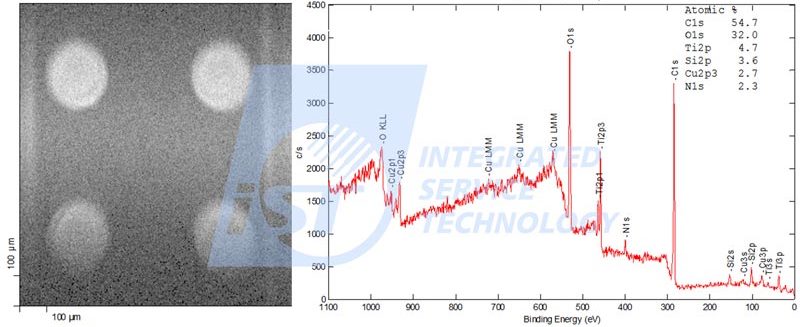
Figure 2: Identify PI surface composition by UBM process with XPS; residuals of C, O, Ti and Si have been found here.
Being an analysis technique that is done by observing electronic beams’ binding energy, the XPS can be used to determine the type of chemical bond by high resolution chemical shift analysis. Take an example. The energy spectrum chemical shift’s curve fitting analysis for the elliptical contaminants on the surface of post-etching Al pad suggest that the contaminant is a coexistence of three chemicals at different binding energies: [AlF6]3- at 78.7eV, AlF3 at 76.3eV and very little Al2O3 at 74.5eV as shown in Figure 3.
The curve fitting analysis technique is ideal not only for products done by the etching process but also for studying the chemical bond ratio of certain ceramic thin films for process improvement and adjustment in the future.
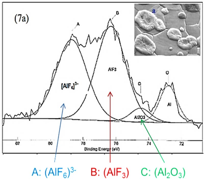
Figure 3: Three chemical bond patterns of corrosion residuals on IC Al pad by XPS: (AlF6)3-, AlF3 and Al2O3. (Courtesy: Y. Hua et al., IPFA 2014).
■ Qualitative analysis of polymer organic compounds in yellow light/etching process – SIMS
TOF-SIMS analyzer, a “time of flight” based secondary ion mass spectrometer for surface analysis at a higher sensitivity, employs an “ion source” for static surface element analysis. Differing from magnetic sector SIMS or XPS for quantitative analysis by dynamic depth profile, the TOF-SIMS employs non-continuous pulse based ion source to bomb the sample surface with less surface energy and fewer charge. With required charge compensation, it is ideal for insulating organic materials analysis.
In case of a sample, by a process relying on polymer organic materials, has been determined by AES, XPS, or other qualitative analyzer that it contains elements including C, N and O, use the mass spectrum analysis based TOF-SIMS to identify its contamination.
Take as an example. TOF-SIMS is a good choice to identify residuals of organic solution, photoresist, or other contamination left by yellow light, etching, or cleaning process.
In addition to the aforementioned qualitative analysis for surface contamination, other surface analysis tools, including atomic force microscope (AFM) and X-ray diffraction based total X-ray reflection (XRR), can be used to probe the surface of ultra-thin (couple-nano thick) film for its surface topography, roughness and thickness. (For more information, please refer to “Precisely measure roughness of sample surface with the help of three tools.”)
II. How Big a Sample is Needed? How Big is the Size of a Foreign Matter or Sample Graph Acceptable for Identification?
How to select a correct analysis tool to deal with anomalies in terms of topography, looks, color or electrical property? Or, select which method to begin with? This differs among the analysis tools as they vary in size of space to hold samples and area of analysis.
Please refer to Figure 4 by iST Surface Analysis Lab to choose the required tool according to the contaminant’s tentative depth and size and desired concentration and flow chart provided.
As shown in Figure 4, let’s assume that the foreign contamination found cannot be observed by a general microscope, and only abnormal discoloration can be identified in one area. Then XPS is your first choice; in case elements C, N, and O were found by the latter, the contamination is very likely organic which, in turn, require FTIR or TOF-SIMS at the bottom of the chart, to determine the exact organic substances of the contaminant.
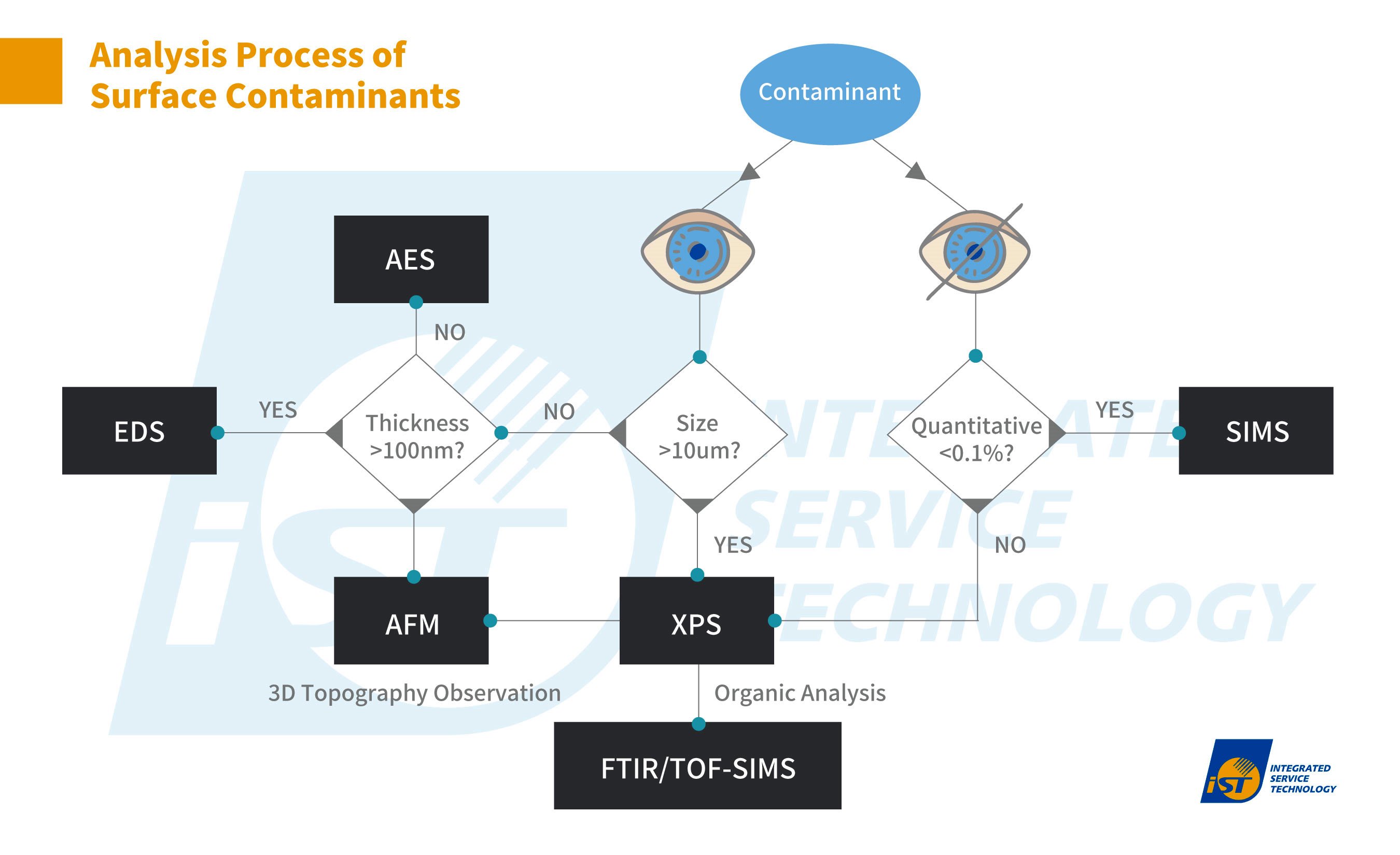
Figure 4: Criteria for selecting a surface analysis tool for surface contamination

This is to share with you our success stories in test and verification. In case it seems hard for you to make a selection and the size of samples fall beyond a given range or you need further information to select the required analysis tools based on the sample size and location of contamination, please mail or call iST to get a copy of the chart designed by us. Please feel free to contact with Mr. Chang at +886-3-579-9909 #6613 │ Email: sa_tw@istgroup.com;marketing_tw@istgroup.com
Other services you may be interested in
surface analysis