Issued Date:2024/1/16 C-AFM defect
Issued By:iST
Even though we can identify hot spots on the chip and spot abnormal Voltage Contrast (VC) in SEM images, pinpointing chip anomalies as we go layer by layer to the bottom remains a challenge. Moreover, due to the SEM’s lack of quantitative electrical measurement functionality, determining whether the abnormality occurred at the P-junction or the N-junction remains unresolved. Let us demonstrate the significant electrical anomalies by using C-AFM to solve your problems.
C-AFM defect

With the rapid advancement of Artificial Intelligence (AI), High-Performance Computing (HPC), and mobile communication, the demand for high performance, low power consumption, and smaller chip sizes is driving swift evolution in process technology, approaching physical limits. As chips are increasingly stacked using 3D packaging technology, the complexity of failure analysis is also growing day by day.
Confronted with highly miniaturized chips, it is sometimes necessary to flexibly utilize various failure analysis tools for defect localization. For instance, when a chip experiences a malfunction, Electrical Failure Analysis (EFA) may identify clear hot spots, but subsequent observations using a Scanning Electron Microscope (SEM) all the way down to the lower layers may still not reveal any defects. This situation often puts research and development engineers in a dilemma.
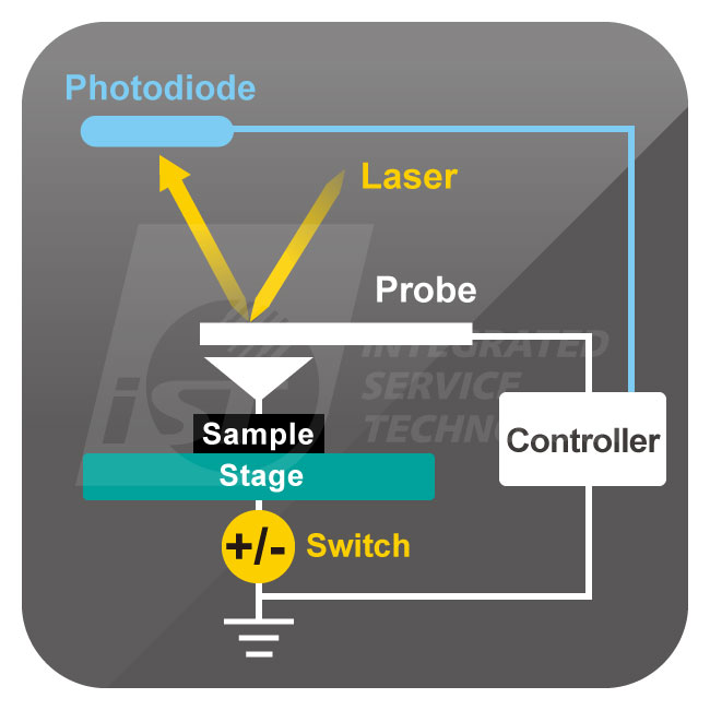
This is precisely when Conductive Atomic Force Microscopy (C-AFM) comes into play. With a 20-year history in measurement field development, C-AFM enables electric current measurement and surface tomography through a single conductive probe with bias condition, whether it’s in the via layer of the back-end metal routing process or the contact layer of the front-end transistor process. C-AFM enables the rapid identification of anomalies by scanning and searching large areas. In this edition of the iST Classroom, we will delve into the operational principles and data interpretation for C-AFM analysis, exploring its powerful and impressive capabilities.
C-AFM defect
C-AFM defect
1. Quick Overview of the Principles and Applications of C-AFM
Speaking of C-AFM, we must first mention its predecessor – the Scanning Tunneling Microscope (STM). STM was invented by two scientists, Gerd Binnig and Heinrich Rohrer, at the IBM Zurich Research Laboratory in Switzerland. They utilized the quantum tunneling effect in the tiny gap between the probe and the sample to detect the surface morphology of materials through the generation of tiny electric currents. This groundbreaking invention earned them the Nobel Prize in Physics in 1986. In the same year, Gerd Binnig, Calvin Quate, and Christoph Gerber modified the probe to utilize Van der Waals’ force between the atoms of the probe and the sample surface. This caused the cantilever to undergo tiny displacements, allowing the depiction of the sample’s surface topography. This marked the development of the Atomic Force Microscope (AFM), and C-AFM is one of its applications.
2. The Ingenious Applications and Optimal Utilization of C-AFM
In most cases, SEM is the primary and excellent tool for identifying the defects from the localizing hot spots. We can use SEM to observe layer by layer to see if any abnormal defects on the metal lines or gate structures of the analyzed chip. Additionally, in the via/contact layer, SEM with built-in Voltage Contrast (VC) effects can also be employed to determine whether the chip is open or leakage. However, SEM lacks the quantitative capability to perform electrical measurement, we still have no idea whether the defect exactly occurred at the P-junction or the N-junction, even when abnormal VC is detected.
Based on the experience of the iST Electrical Failure Analysis Laboratory, it is sometimes challenging to isolate the leakage fault from the gate to the N-junction of the NMOS through SEM VC analysis due to the inherent structure of NMOS, as shown in Figure 1(a) SEM image. However, C-AFM utilizes bias voltage applied on the sample stage and measures current through the conductive scanning probe, which enables scanning a large area for the detection of defects. Hence, a rapid determination for leakage or open electrical anomaly at a specific location connected to the P-junction, N-junction, or the bulk is achieved. C-AFM is analogous to the “rapid tests” for testing the COVID-19 in electrical characterization for failures. For more precise “PCR nucleic acid testing”, we can further use Nano Prober (read more: Methods of precise positioning for defect detection based on nanoscale electrical characteristics measurement) to accurately localizing the hot spot and electrical characterization. Subsequently, material analysis can be performed using techniques such as Dual-Beam FIB (DB-FIB) or Transmission Electron Microscopy (TEM) to reveal the physical anomaly that caused the chip malfunction. The obtained electrical data enables the interpretation on the observed defect in the subsequent material analysis for the further root cause investigation.
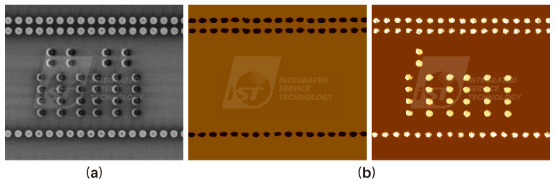
Figure 1: The leftmost grayscale image (a) is an SEM display image, while the two images on the right are (b) C-AFM current maps. The electrical states of the sample can be interpreted from the black spots or white spots in these images.
(Source: iST)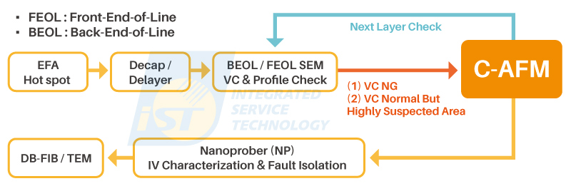
Figure 2: The optimal timing for C-AFM measurements in the failure analysis process.
(Source: iST)3. How to Interpret C-AFM Data Rapidly
Interpreting C-AFM data is not difficult, as long as you understand the bias characteristics of a PN diode. When applying a positive voltage to the P-region and a negative voltage to the N-region, current flows from the P-region to the N-region. This voltage condition is defined as forward bias, as shown in Figure 3(a). Conversely, when the polarity is reversed, creating a negative voltage on the P-region and a positive voltage on the N-region, it is termed reverse bias, as depicted in Figure 3(b), and no current flows through the PN junction with such bias condition.
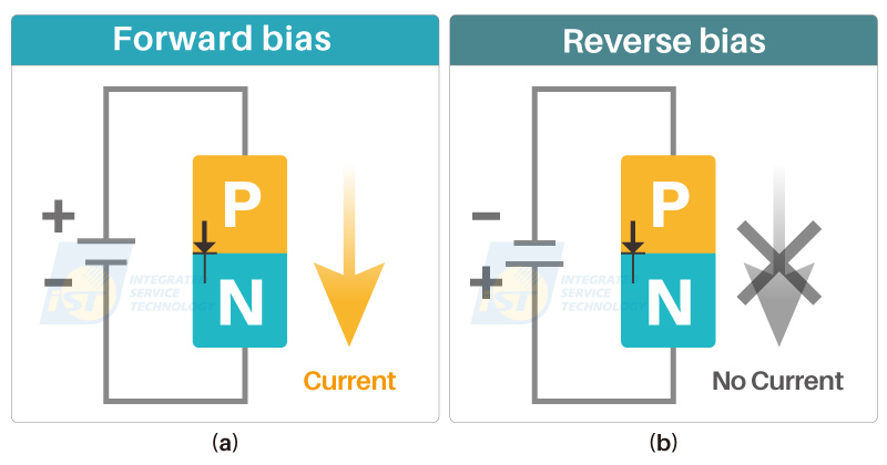
Figure 3: (a) Schematic diagram of forward bias;
(b) Schematic diagram of reverse bias.
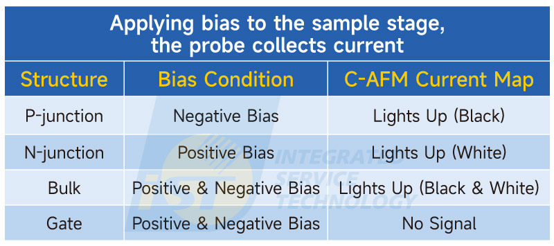
(Source: iST)According to the machine operation configuration, the bias is applied from sample backside. Applying a negative bias to the sample allows the probe to sense and label the position of the current, presenting a black signal in the current map. Conversely, applying a positive bias to the sample results in a white signal in the current map. From the current examples in Figure 4, it can be observed that when a negative bias is applied to the sample, the contact connected to the P-junction lights up in black (Figure 4(a)). Conversely, when a positive bias is applied to the sample, the contact connected to the N-junction lights up in white (Figure 4(b)). Here, iST Electrical Analysis Laboratory has compiled a C-AFM data interpretation table for your reference (Table 1).
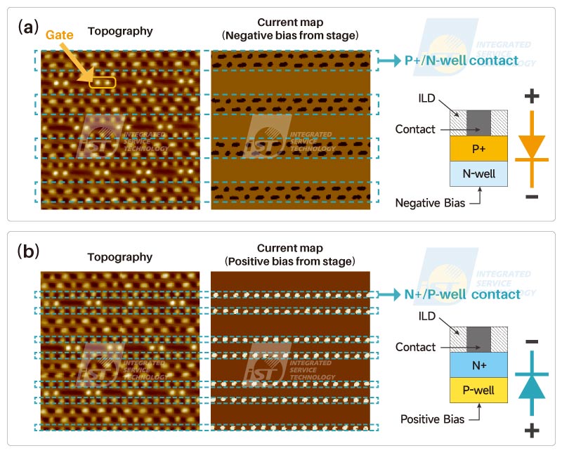
Figure 4: (a) Applying a negative bias to the sample backside, P-junction contact lights up (black);
(b) Applying a positive bias to the sample backside, N-junction contact lights up (white).
(Source: iST)Table 1: This table serves as a quick reference for interpreting the meaning behind C-AFM data.
(Source: iST)
4. Four Major Case Studies of C-AFM
By combining abnormal current map with I-V curve measurements (current-voltage curves) in C-AFM, it is possible to identify failure modes such as Open, Short, Leakage, and even High Resistance failures. The explanations for these four modes are as follows.
(1) Open Mode
For a normal PMOS, the P-junction is biased negatively to allow conduction, and the current map appears black. The reference (Ref) position for the I-V curve is indicated by the green line in Figure 5(b), corresponds to this normal condition. However, due to an open fail at the Via 2 in the Target position, preventing current flow through the PN junction, there is no signal in the current map at Via 3. The I-V curve for the Target position is represented by the orange line in Figure 5(b).
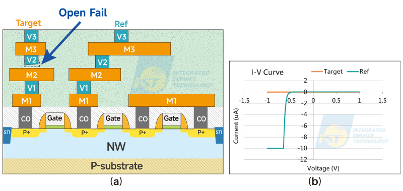
Figure 5: (a) Schematic diagram of process open circuit failure;
(b) I-V curve results from C-AFM.
(Source: iST)(2) Short Mode
For a normal PMOS, the P-junction is biased negatively to allow conduction, and the current map appears black. The I-V curve is represented by Ref 2 (deep green dashed line) in Figure 6(b). Similarly, for a normal NMOS, the N-junction is biased positively to allow conduction, and the current map appears white. The I-V curve is represented by Ref 1 (light green dashed line) in Figure 6(b).
In figure 6(a), there is a short fail between Target 1 and Target 2 at Metal 2 layer. Signals from both the P-junction and N-junction received in the I-V measurements at Via 2 is caused by the short failure. The overlapped I-V curves for Target 1 and Target 2 are depicted by the orange and yellow lines in Figure 6(b), respectively. The current map at Via 2 simultaneously receives signals appearing both black and white.
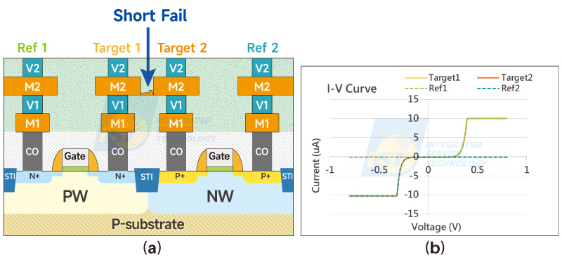
Figure 6: (a) Schematic diagram of process short circuit failure;
(b) I-V curve results from C-AFM.
(Source: iST)(3) Leakage Mode
A normal gate structure will not register any current map signals in C-AFM, as depicted by Ref (green line) in Figure 7(b). In Figure 7(a), the Target Gate with a black spot on current map illustrates gate leakage to the P-junction from C-AFM analysis. The subsequent I-V measurement also provide quantitative leakage information of gate leakage, as shown by the orange line (Target) in Figure 7(b).
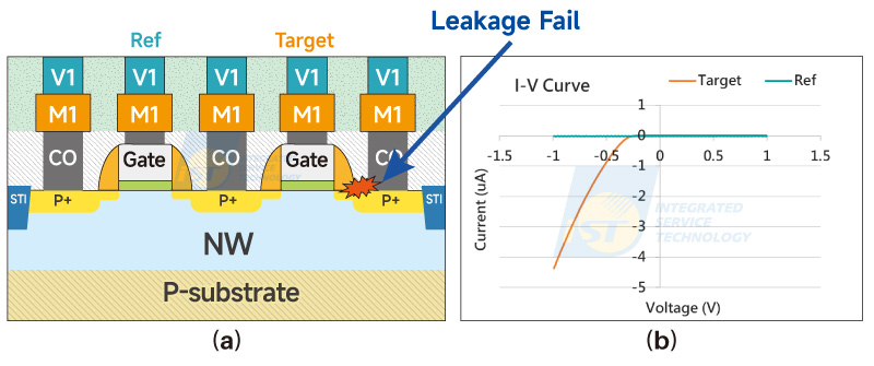
Figure 7: (a) Schematic diagram of process gate leakage failure;
(b) I-V curve results from C-AFM.
(Source: iST)(4) High Resistance Mode
For a normal NMOS, the N-junction is biased positively to allow conduction, and the current map appears white. The I-V curve is represented by Ref (green line) in Figure 8(b). In Figure 8(a), the defect in the Target region exhibits incomplete connection to Metal 2 at Via 2. In the C-AFM current map at Via 3, a lighter shade of white is observed compared to Ref, and its I-V curve (depicted by the orange line) demonstrates high-resistance characteristics (Figure 8(b)). For certain cases, it is still hard to have significant contrast from current map on high resistance failure. But we can still distinguish the failure from I-V measurement from C-AFM, or further Nano prober analysis.
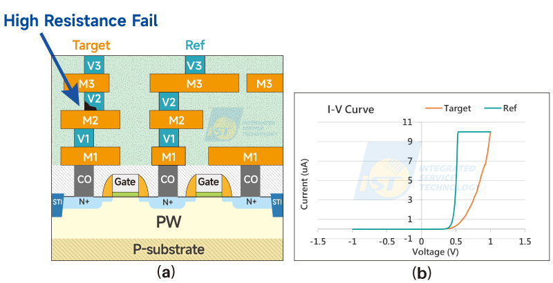
Figure 8: (a) Schematic diagram of process high resistance failure;
(b) I-V curve results from C-AFM.
(Source: iST)
Through today’s iST classroom introduction, we hope to bring you to have a deeper understanding of the powerful capabilities of C-AFM. With applying C-AFM, the failure analysis coverage for the analyzed failures will be greatly enhanced to solve the blind-spot from SEM analysis (Figure1) and provide “rapid test” on quantitative electrical characterization before thoroughly characterization by Nano Prober.
If you are interested in exploring other applications of C-AFM, feel free to refer to our previous iST classroom articles (Read more: Where to seek help for CIS chip defects?)). Discover how C-AFM is applied in the failure analysis of CMOS image sensors (CIS) with thin structures and unique 3D stacking features.
This article is shared with all of you, our long-standing supporters of iST. If you would like to explore further details, please feel free to contact
Ms. Hsu at +886-3-579-9909 ext. 6699 or via email at EFA@istgroup.com ;marketing_tw@istgroup.com