Issued Date:2023/10/17Thin film adhesion hardness
Issued By:iST
Resolving the issue of diverse material mechanical properties in advanced packaging technology involves the crucial utilization of nanomechanical indentation and scratch testing. However, how to combine them with SEM & TEM to pinpoint defects?
Thin film adhesion hardness
In the realm of semiconductor integrated circuits, where the focus is on shrinking dimensions while maximizing functionality, advanced packaging technology has emerged as a crucial avenue for enhancing chip performance. However, to achieve vertical integration, the use of multilayered thin film stacking structures has become widespread in the manufacturing process. Yet, due to the mismatched mechanical properties of different materials and the thermal-mechanical stress generated during production, a host of failure modes have emerged.
To surmount these challenges, mastering the mechanical properties of materials has become paramount. In the micro and nano world, two crucial analysis tools step forward: the “Nanomechanical Indentation Tester” and the “Nanomechanical Scratch Tester.” Beyond just analyzing material mechanical characteristics and the adhesion capabilities within multi-layer structures, they serve as tools to assess localized stress. When coupled with subsequent image analysis techniques like Scanning Electron Microscopy (SEM)、Dual Beam FIB or Transmission Electron Microscopy (TEM), enabling a deeper exploration of internal structural changes, helping pinpoint fragile locations responsible for malfunctions.
In this edition of the iST classroom series, in collaboration with Anton Paar, we delve into the principles and applications of nanomechanical indentation and scratch testing. The aim is to shed light on these techniques that hold the potential to decipher the challenges posed by advanced packaging technology and aid engineers in their pursuit of robust semiconductor designs.
Thin film adhesion hardness
Thin film adhesion hardness
1. The Principles of Nanomechanical Indentation and Scratch Tester
Nanomechanical testing methods, such as nanoindentation and scratch testing, are widely used techniques to study the mechanical properties of materials at micro and nanoscales. These methods help us understand how materials deform or fracture under stress at these small scales. Compared to traditional testing methods like Vickers or Rockwell hardness tests, nanoindentation and scratch testing provide more detailed information, offering multiple characteristic parameters beyond just a single hardness value. (Read more: Key to heterogeneous integration: Materials Bonding Stress)
The nanoindentation tester features a precise stress and depth sensor that enables accurate control of the loading and unloading process of the indenter. Simultaneously, it records the applied load and the depth of indentation. This allows us to extract various material parameters related to indentation depth, such as “hardness(HIT)” that represents a material’s resistance to permanent deformation, “elastic modulus(EIT)” describing material elasticity, and “creep behavior(CIT)” indicating material deformation under a constant load.
Scratch testing, on the other hand, is employed to measure the adhesive strength between thin films and substrates or within thin films themselves. By incrementally applying force to a diamond tip on the surface of the material, shear forces are generated. When the mechanical properties of the thin film and the substrate differ, adhesive failure occurs at a “critical load (Lc)” value. This critical load is a vital quantifiable parameter that reflects the film’s adhesion capability. In a single scratch test, materials with higher critical loads exhibit better adhesion, offering enhanced resistance to thermal stress impacts during subsequent processes.
Figure 1: Operation of nanoindentation tester/scratch testing equipment.
2. Four Key Applications of Nanoindentation and Scratch Testing Instrument in Semiconductor Engineering
(1) Investigating Multilayer Film Delamination through Nano- Scratch Testing
In the pursuit of advancing 3D IC packaging technology, semiconductor devices have evolved towards a highly multilayered structure—stacking various thin film materials with distinct characteristics. However, the phenomenon of “interfacial delamination” occurs frequently during the manufacturing process due to thermal and mechanical stresses from different processes. This is mainly caused by the mismatch in mechanical properties between thin film/ thin film or substrate/ thin film interfaces, such as differences in coefficients of thermal expansion (CTE), Young’s modulus, or Poisson’s ratio. This delamination at interfaces has become a common cause of device failure.Thin film adhesion hardness
To address this challenge, understanding the adhesion between materials and how structures react under external stress becomes crucial. Nanoindentation and scratch testing instruments offer an ideal analytical approach. They not only quantify the forces causing interfacial delamination but also apply stress to simulate material failure due to external forces. Moreover, after interfacial delamination occurs, combining techniques like Scanning Electron Microscopy (SEM)、Dual Beam FIB or Transmission Electron Microscopy (TEM) can further analyze changes in the multilayered internal structure and pinpoint the weaker points.
Taking the Si/SiO2(SiN)/TiN/W multilayer structure shown in Figure 2 as an example, a diamond tip with a 2-micron diameter was used to create scratches on the surfaces of two different multilayer samples using a loading rate of 2 mN/s (as shown in Figure 2). Analysis of the data from the scratch testing instrument revealed that the critical loads for Sample A and Sample B were 7 mN and 15 mN, respectively. This indicates that Sample B has better resistance to external stress. Additionally, compositional distribution analysis using Transmission Electron Microscopy (TEM) and Energy-Dispersive X-ray Spectroscopy (EDS) mapping indicated that interfacial delamination occurred at the SiO2/TiN and SiN/TiN interfaces of these two structures [1].
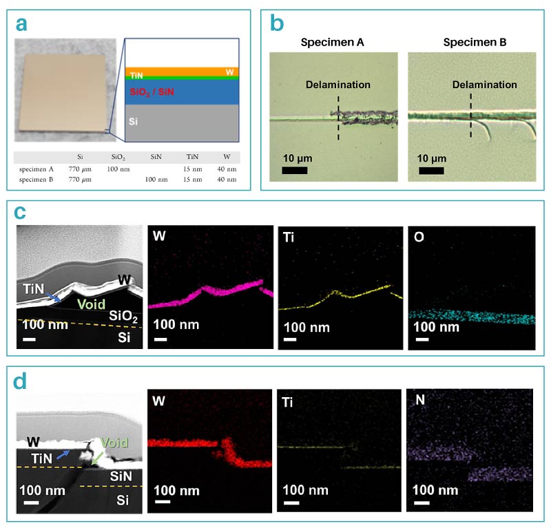
Figure 2: (a) Schematic diagram and explanation of the multilayer structure.
(b) Interfacial scratch and delamination for different samples. (c) TEM and EDS mapping analysis results for the multilayer Si/SiO2/TiN/W Sample A. (d) TEM and EDS mapping analysis results for the Si/SiN/TiN/W Sample B. [1](2) Mechanical Characterization of Copper Pillar Bumps
To meet the demands for smaller, thinner, and more compact end products, the quantity of signal processing input and output in chips has been continuously increasing. This implies a need for higher wire node density in chip packaging and shrinking distances between the bumps that connect chips and substrates. Copper, with its advantages of low resistance, low inductance, low thermal resistance, and electron migration resistance, has emerged as an excellent choice for achieving close spacing, leading to the utilization of Copper Pillar Bumps (Cu Pillar Bumps).
However, when the spacing between these bumps decreases to around 10 micrometers, several challenges arise [2]. For instance, the Copper Pillar Bump structures encounter issues like “Bridge Failure” due to thermal stress during the reflow process.
To address these challenges, a nanoindentation testing instrument equipped with a microscope lens can be employed. Nanoindentation experiments can be conducted at specific locations on the copper pillars, allowing for mechanical property analysis in different regions and process parameter optimization. Figure 3 illustrates copper pillar bumps prepared using high-speed electroplating methods[3], coupled with different process approaches and nanoindentation experiments. This combination enables the understanding of the impact of current density (denoted by the symbol “j”) during electroplating on the mechanical properties of copper pillars. As shown in Figure 3(b), there is a positive correlation between the hardness of the copper pillar and the applied current density(j) during the electroplating process.
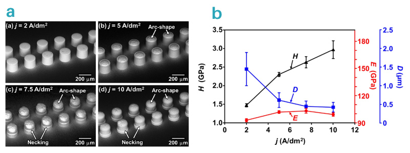
Figure 3: (a) SEM images of copper pillars produced through electroplating processes with different current density(j). (b) The relationship between hardness of copper pillar, elastic modulus, and electroplating current density(j).
(3) Analysis of Mechanical Compatibility Between Underfill Material and Bumps
In the process of IC flip chip packaging, an underfill material is injected between the bumps to enhance the mechanical stability of the chip and improve overall reliability. Underfill materials are typically high-polymer substances with significant differences in Young’s modulus and CTE when compared to the surrounding copper pillar bumps and the underlying silicon substrate [4]. Due to this mechanical mismatch, various failure modes may occur during subsequent high-temperature and high-humidity reliability tests, such as crack formation, substrate separation, and voids.(Read more: How to Eliminate Underfill Voids with Vacuum Pressure Oven)
To identify the main causes of these failures, it’s crucial to analyze the differences in mechanical properties at various positions within the structure. In recent years, nanoindentation testing instruments have been widely used to measure the mechanical properties at different locations within structures. Figure 4(a) illustrates a cross-sectional view of an underfill structure after filling, and using the optical microscope equipped with nanoindentation, three different regions are selected for analysis: copper pillar bumps, underfill material, the backend process chip, and the silicon chip.Thin film adhesion hardness
From the results in Figure 4(b), the uneven distribution of Young’s modulus indicates the presence of additional fillers in the underfill. Figure 4(c) displays the distribution of the elastic modulus at the interface between the copper pillar bump and the chip. By performing indentation tests at specific positions, the Young’s modulus of the silicon wafer, copper pillar bumps, and underfill can be determined. As shown in Figure 4(d), they are 169 ± 3 GPa, 119 ± 6 GPa, and 9 ± 3 GPa, respectively [4]. This outcome reveals that the significant modulus difference increases the risk of failures in the structure due to subsequent processes.
Thus, in combination with the results from the indentation testing instrument, it’s possible to effectively find optimized process parameters or change materials with different properties to avoid product failures caused by mismatched mechanical characteristics.
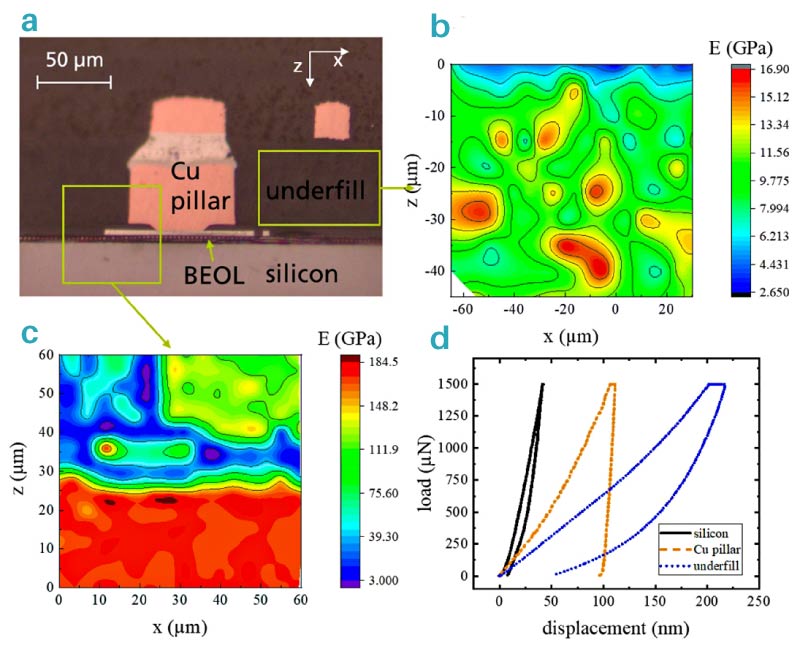
Figure 4: (a) Different experimental regions for nanoindentation. (b) Elastic modulus distribution map of the underfill region. (c) Elastic modulus distribution map at the interface of the copper pillar bumps. (d) Nanoindentation load-displacement curves.
(4) Analysis of Hardness and Adhesion Relationship in Passivation Protective Layers
In Wafer Level Package (WLP) structures, various deposition methods are used to create active devices like transistors on the substrate. Different layers are stacked above the substrate, including metal layers, redistribution layer (RDL) for circuit rewiring, metal pads for circuit connection, and passivation protective layers [5]. The primary purpose of passivation layers is to shield the underlying structures from external contamination or damage. Different deposition methods or process conditions significantly impact the mechanical properties and adhesion of passivation layers to the substrate. Combining results from nanoindentation and scratch testing instruments not only helps identify the relationship between mechanical properties and adhesion but also accelerates process optimization and material selection for protective layers, thereby expediting subsequent development processes.Thin film adhesion hardness
Taking silicon nitride (SiNx) thin films as an example, Figure 5(a) shows load-displacement curves of approximately 300 nmthin films deposited on silicon wafers using two different processes. The results reveal that Layer 1 has a higher hardness than Layer 2. However, further analysis using the scratch testing instrument for adhesion indicates that interface delamination was observed in Layer 1 at lower loads, while under the same conditions, no interface delamination was observed in Layer 2. This result suggests that the adhesion of Layer 2 is superior to that of Layer 1.
Interestingly, when comparing the results from the nanoindentation tests, it becomes evident that although Layer 1 has higher hardness, its adhesion is not better. From this, it’s apparent that the presentation of a thin film’s mechanical properties and adhesion isn’t always positively correlated. Thus, a comprehensive approach considering both aspects is necessary to determine the optimal material characteristics.
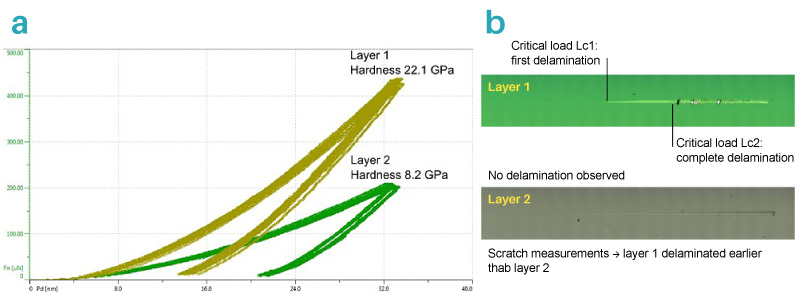
Figure 5: (a) Load-displacement curves of approximately 300nm SiNx thin films deposited on silicon wafers using two different processes. (b) Scratch testing images of the two SiNx thin films. (Image source: Anton Paar)
In recent years, as packaging technology continues to evolve, the conventional approach of using single large-area materials no longer fits the requirements of complex 3D structures. The trend towards combining, aligning, or stacking chips of different sizes within tiny spaces has become more evident. However, in these minuscule structures, the interaction of heterogeneous materials is subject to complex mechanical stresses after packaging. As a result, apart from the need for precise microscale mechanical property measurement capabilities, the integration of imaging-based techniques such as Scanning Electron Microscopy (SEM)、Dual Beam FIB or Transmission Electron Microscopy (TEM) has become essential for analysis. In the development of advanced packaging technology for future ICs, iST will continue to collaborate closely with all our clients to research and develop more efficient next-generation chips. This collaborative effort aims to make our future lives more diverse and vibrant.Thin film adhesion hardness
This is to share knowledge and experiences of iST with you. Should there be any inquiry or if you would like to know more about the aforementioned techniques, just ring Neal Chiang at +886-3-579-9909 Ext. 6176 or email him at web_sa@istgroup.com;marketing_tw@istgroup.com。
References:
[1] Jin-Hoom Kim, Hye-Jun Kil, Sangjun Lee, Jinwoo Park, and Jin-Woo Park. ACS Omega 2022, 7, 25219−25228.
[2] https://technews.tw/2022/07/29/ma-tek-package-design-hybrid-bonding/
[3] Pei-Tzu Lee, Chih-Hao Chang, Cheng-Yu Lee et al. Materials & Design 206 (2021) 109830 “High-speed electrodeposition for Cu pillar fabrication and Cu pillar adhesion to an Ajinomoto build-up film (ABF)”
[4] Thesis with the title “Micromechanical indentation study of stress related effects in transistor channels” by Simon Schlipf
[5] 中華民國專利,申請案號:102121292