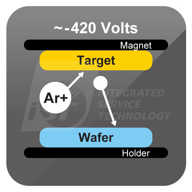
During the phase of wafer thinning, the front-side metal sputtering deposition of front-side metallization process is to dissociate argon atoms (Ar) in a high vacuum environment to give secondary electrons and Ar ions, accelerate the latter with the negative potential on the target to hit the target and deposit target metals on the surface of the wafer.
Metal Sputtering Deposition Process
Customers’ wafers shall be fed into sputtering machine for metal deposits according to given metal types and thicknesses after IQC; subject the deposited wafer to metal etching after defining the metal via photo aligner with the customer-specified mask pattern and photolithography machine; perform OQC after PR (photoresist) strip.
The Superiority of iST
- Minimize loss of thickness of the exposed Al pad with Ti / NiV / Ag based high selectivity rate matching for customers proceeding with mix bonding at lower package costs in subsequent processes.
- Teams of photolithography specialists are ready any time to help customers review Tape Out / Job Files for painless transfer of subsequent masking.
- A team of engineers with diversified experts including front end wafer foundry, wafer thinning and backend packaging house, knowledgeable and experienced in process integration and analysis in phases from front through middle to back and well-prepared to assist customers in accelerated development, troubleshooting, and mass production stabilization.
Case Sharing
- Existing metal options: Ti / NiV / Ag with thickness subject to customer requirements.
- Applicable to 8" wafers.
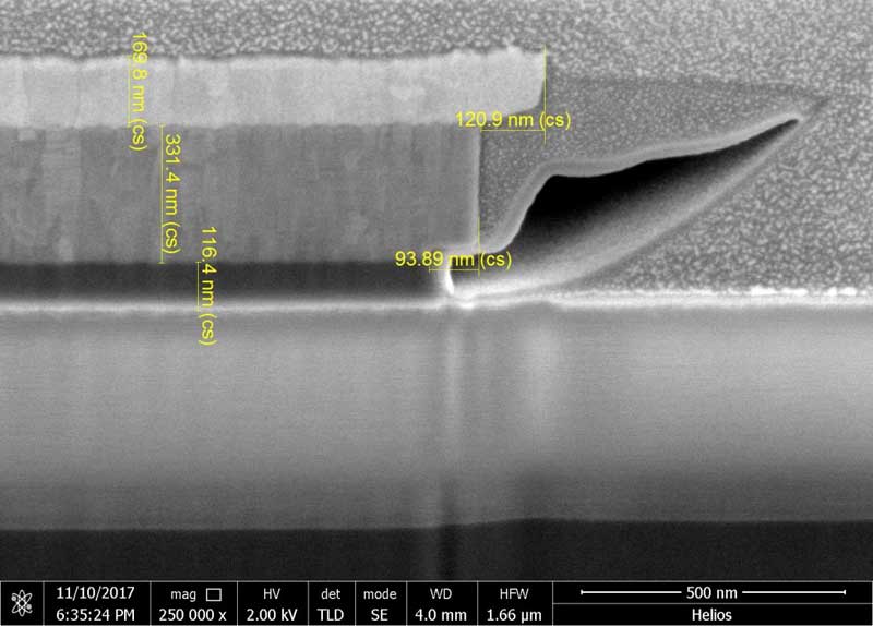
- Excellent uniformity of Ti/NiV/Ag growth.
- Minimum undercut.


