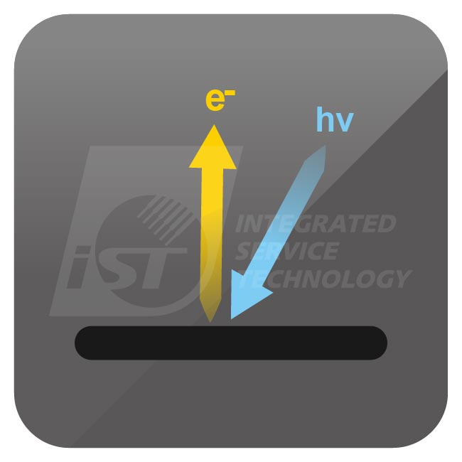
XPS is based on the principle of the photoelectric effect. Electrons within the inner layer of atoms are excited into photoelectrons once an X-ray penetrates a sample. Photoelectrons close to the material surface will escape the surface and get detected by the instrument which can be used to identify the composition of surface elements and determine their chemical bonds.
What iST can do for you?
XPS is capable of obtaining information of surface element distribution and chemical bonds, and the analysis is not affected by conductivity of the sample.

The Superiority of iST
The high resolution XPS – Quantera II Scanning X-ray Photoelectron Spectroscopy acquired by iST is capable of micro area analysis as fine as 7.5um, compared to the 50um capability of conventional XPS, offering more refined structure analysis of sample surface that can satisfy industry needs.
Case Sharing
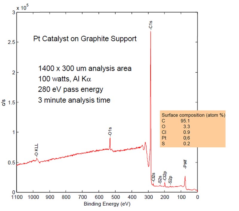
Pt Catalyst on Graphite Analysis
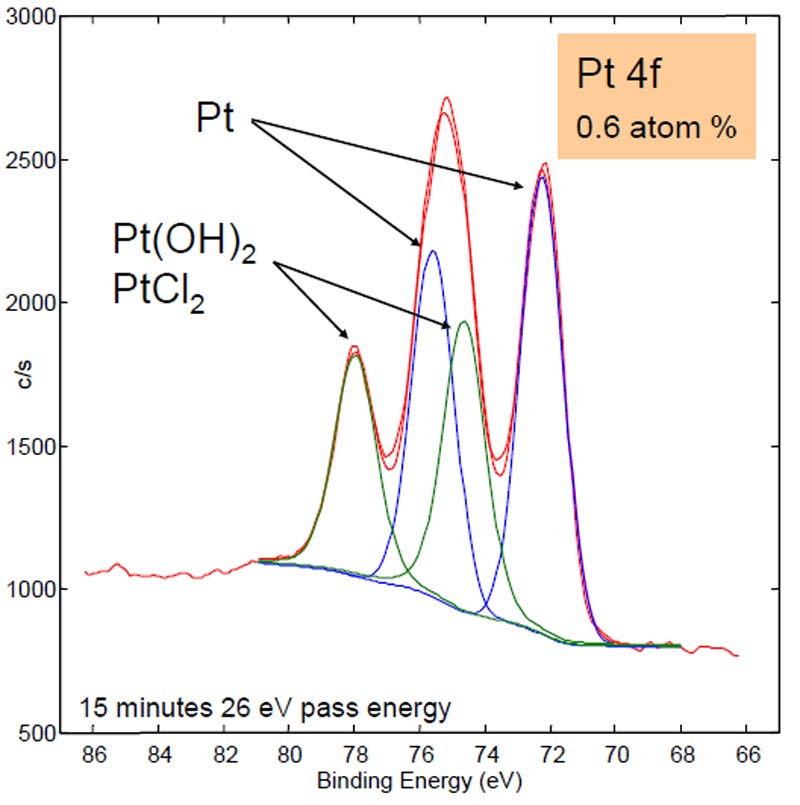
Narrow scan EDS of Pt 4f
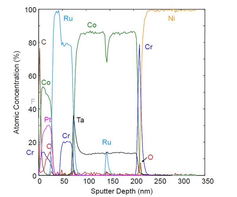
Depth Profiling of hard drive disc
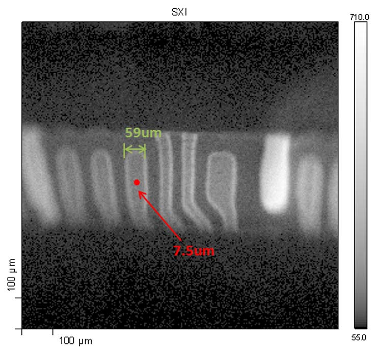
Gold finger on IC substrate analyzed by SXI
(Beam size : 7.5um)
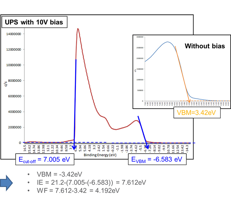
WF & IE calculation
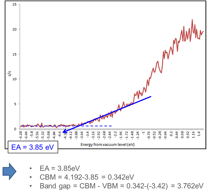
EA calculation
- Surface Survey: Ingredient Analysis Of Material Within 100A On Surface Of Sample
- Narrow Scan: Chemical Bonding Configuration Analysis Within 100A On Surface Of Sample
- Oxidation Analysis Of Sample (Oxidation Depth And Oxidation State)
- Depth Profile Analysis: Via Ar Ion Sputtering Of Sample Surface, Acquire Signals Of Elements At Different Depths In The Vertical Profile.
- Spectrum Mapping: Analyze Specimen Zonal Element Signals For Acquiring Zonal Elements Distribution Image.
- Line Scanning: Analyze Linear Element Signals Of Specimen For Acquiring Linear Element Distribution Map.
- Ultraviolet Photoelectron Spectroscopy (UPS): Analyze Valence band structure and Work function .
- Low Energy Inverse Photoemission (LEIPS): Analyze Conduction band structure and band gap (combined with UPS) .
- Gas Cluster Ion Beam (GCIB): High performance for depth profiling many polymer and organic films while minimizing the potential for chemical damage .
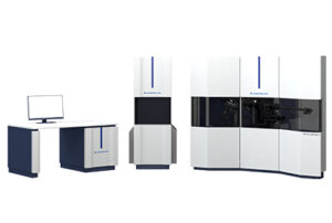
PHI Quantera II
- X-ray minimum spot size: 7.5um
- Energy Resolution: 0.48 eV (Ag3d5/2)
- Specimen Positioning: SPS optical and SXI imaging
- Specimen size:<75mm
PHI Quantera II
- X-ray minimum spot size: 10um
- Scanning Auger Microscopy Option (SAM)
- 20 kV Ar Gas Cluster Ion Beam Gun Option (GCIB)
- UltraViolet Source Option (UPS)
- Low Energy Inverse Photoemission Option (LEIPS)
In semiconductor, LED, PCP and panel manufacturing industry, surface element survey plays a vital role in product development and production monitoring.
Contact Window | Ms. Wu/Ping | Tel:+886-3-5799909# 6183/6177 | Email:web_ma@istgroup.com