Issued Date: 2018/11/20
Issued By: iST
You may know that you can use reverse engineering to understand IC design architecture to avoid patent disputes, but do you know which reverse engineering device you would employ to perceive a nano-scale IC circuit?
Among those unfamiliar with reverse engineering, it’s common to deem it the same as hacking, piracy, and only protects your own technologies from being used by competitors illegally but also prevents you from infringing the patents of your rivals.
Manufacturers in the semiconductor industry have been using reverse engineering as the main tool for IC R&D. The reverse engineering technique is assisting IC design houses in analyzing costs, man hours, talent, and technology required for new product development by extracting circuit to compare the latter against patent map databases, which is not only to evade the patented circuits of others but to get a better understanding of market status and exploitation of opportunities.
Earlier IC reverse engineering depends on photographing the circuit with an optical microscope (OM) to look into IC circuit design. This is not the case when the width of the smallest ‘feature’ on semiconductors keeps on shrinking from 28 nm, 16 nm, 10 nm, 7 nm, 5nm through to even smaller scale as fully-auto photo stitching by OM is limited to a zoom rate of 1500 or smaller. This is unable to present clear circuits on chips.
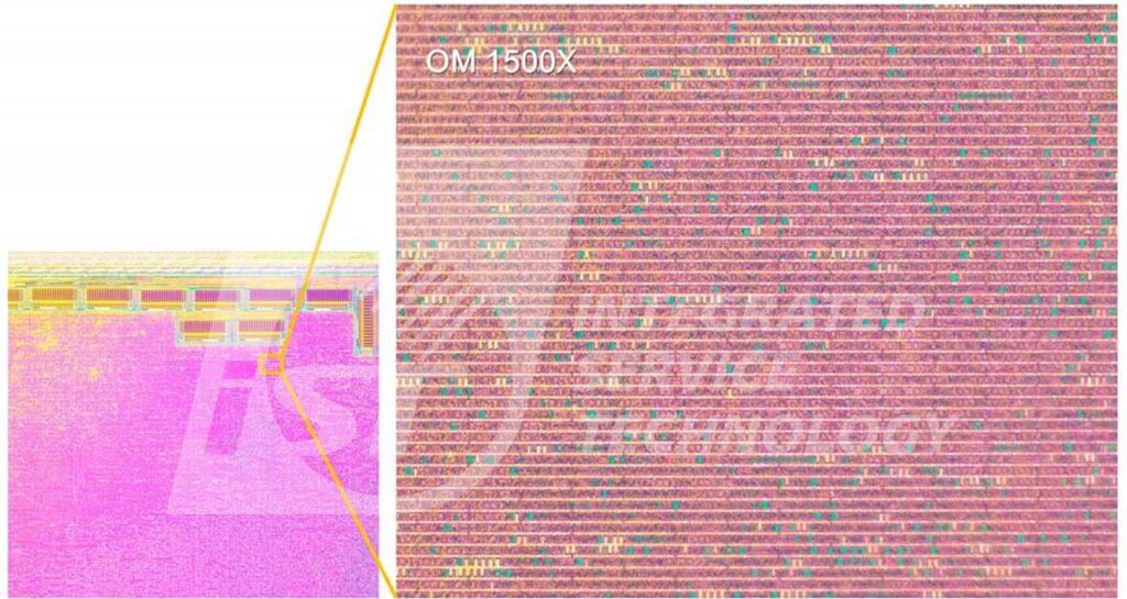
Description: This is a chip image by OM at a zoom rate of 1500; the one on the left side is mosaicked by 1000 OM photos; the one on the right is an enlarged part from the left which is too coarse to give a meaningful nano-grade circuit image.
For nano-grade circuits, you need a scanning electronic microscope (SEM) which can zoom up to 40K in case of large area scanning-shooting-stitching and 1 million for local shooting.
SEM functions in two ways: the first is to find product defects with failure analysis which requires “local shooting”; the other is large area scanning photography to perceive entire circuits in IC. This article aims to review the latter for IC reverse engineering to avoid patent issues by good patent evasion.
The latest SEM machine introduced by iST can work with photo stitching software for large area scanning and photographing IC to unveil circuit design by zooming at a 40K rate.
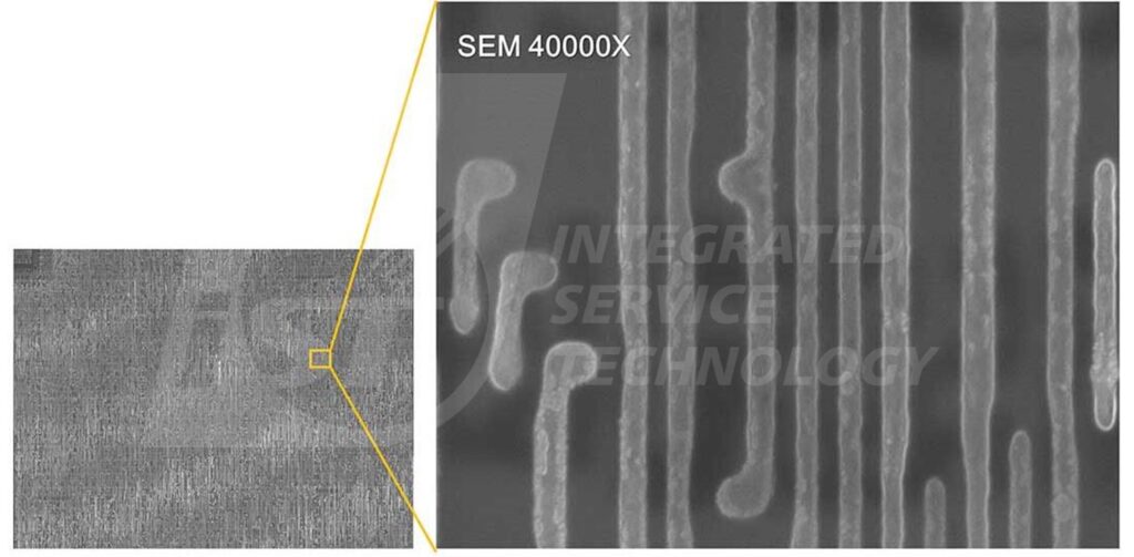
Description: This a chip image by SEM; the one on the left side is mosaicked with 100 SEM photos; the one on the right is an enlarged part from the right which shows the nano-grade circuit image clearly.
Please be reminded that iST can provide an image with SEM large area scanning photography and required software for you to 1. Pan and zoom while viewing it; 2. Measure its dimensions; 3. Identify the relationship between individual metal circuit diagrams.


Description: Viewing images with software provided by iST to pan and zoom at your own discretion and display images of nano-width circuits (upper left, upper right, lower left) along with dimension measurements (lower right)


Description: With stacked delayer and SEM photo stitching, customers may view the relationship between individual metal layers with iST software.
This article is aimed to share our experiences with honorable clients like you. In case you want to know more details, please call Mr. Chen at +886-3-579-9909 Ext. 6641 or email: web_pfa@istgroup.com
* Note 1: Photos of IC illustrated in this article is a market available one and not a sample from an iST customer.
* Note 2: IC samples from our customers are kept strictly confidential by iST. In no case shall iST disclose the analysis outcomes of customer samples to any others.