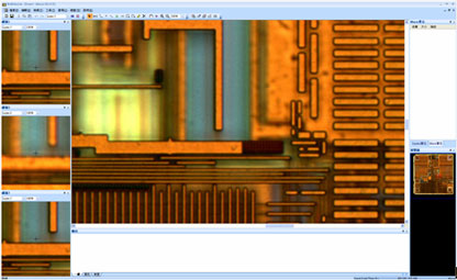
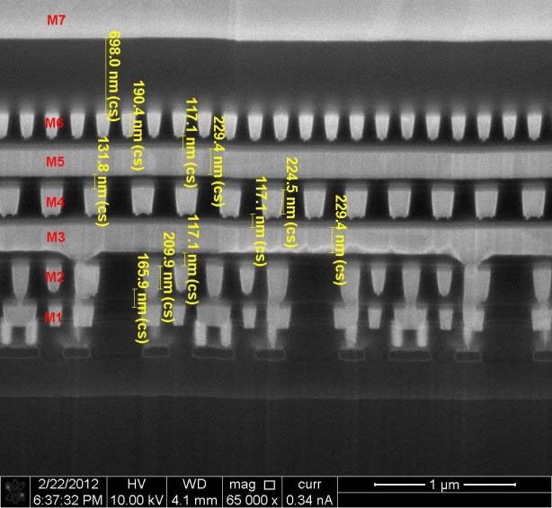
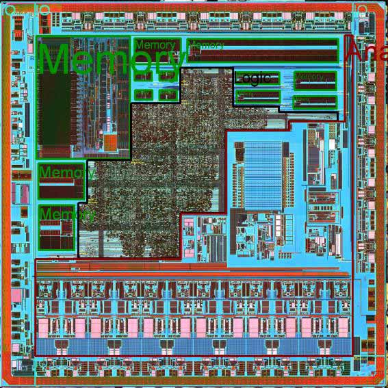
Through the photography system of microscopy, the structure texture of the chip layers can be presented in digital photos. The surface of a large area can be shown through stitching sequence images (iST has developed proprietary software that enables customers to observe circuits in different layers.
The Superiority of iST
With respect to competitive analysis, iST may help you with more design creativity, shorter design cycle, and improved design quality with its "total integrated analysis process and professional service."
Case Sharing
| Metal Material | Cu Metal |
|---|---|
| Process Layer | 1P 7M + 1 Al Top Metal |
| Top Metal(M8) Thickness | 2.98um(min) |
| M7 Thickness | 3.57um(min) |
| M6-M2 Thickness | 190.4nm(min) |
| M1 Thickness | 158.9nm(min) |
| M1 Pitch | 233.8nm(min) |
| CNT Size | 91.2nm(MAX) |
| Poly Size | 60.0nm(min) |
| Comment | Possibly chip process could be 1P7M /65nm with Cu Metal and 1 Al Top Metal |
- IC Package Analysis : Package type/ External appearance/ Internal structure X-ray inspection
- IC Physical Structure : Die appearance/ Metal material analysis/ Process Analysis
- Circuit Module Analysis: Proportion of Circuit Structure (Analog Circuit, Input/Output Circuit, Logic Circuit, Memory Circuit), Memory Package Form, Memory Capacity
- Parameter Measurement of IC Package: Package Size, thickness of leadframe, Wire Bonding Width, Loop Height of Wire Bonding, Material of Epoxy and Wire
- Circuit Layout Structure and Layer Analysis of BGA substrate
Contact Window|Mr. Peng/Amos|Tel:+886-3-5799909#6762|Email:web_reverse@istgroup.com


