Dual Beam Functionality
iST’s Dual Beam FIB systems integrate Ga-ion beam with scanning electron microscopy (SEM) for performing precise sample cleaving and high-resolution imaging simultaneously. We may use FIB for site-specific sputtering or deposition to prepare samples for TEM analysis, develop nanoscale prototypes, or alter circuits with precision down to 14 nm.
Thus, we may also examine the sample in real-time using the SEM for detailed secondary electron images of its topography and composition. This dual functionality allows “slice and view” for 3D microstructure reconstruction, in-situ lift-out for TEM sample preparation, and elemental mapping with EDS. It shows our ability to study materials at the atomic level.
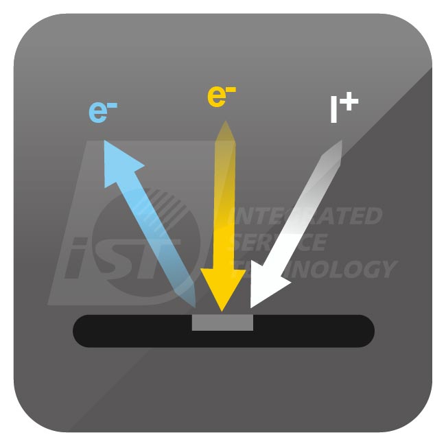
The dual-beam FIB equipment is capable of simultaneously imaging the cross section by electron beams while cleaving the sample with ion beams. As well as performing the EDX composition analysis.
Contrast with Single-Beam FIB
- Integration of SEM and FIB: In single-beam FIB, imaging is limited to ion-induced secondary electrons. On the other hand, Dual Beam FIB integrates SEM, which allows us to capture high-resolution electron images simultaneously while sputtering with the ion beam. It heightens our analytical capabilities and efficiency.
- Simultaneous Imaging and Milling: With single-beam FIB, sequential operations are necessary for imaging and milling. However, Dual Beam FIB enables simultaneous imaging and milling. It accelerates our sample preparation and analysis process and provides us with real-time adjustments to our approach.
- Enhanced Material Deposition: Single-beam FIB systems deal with ion-induced material deposition but lack precision. With its SEM component, the Dual Beam FIB improves our precision in the material deposition while allowing us to observe the deposition process in real time. It offers higher accuracy in nanofabrication tasks.
- 3D Reconstruction Capabilities: Although single-beam FIB can perform sequential sectioning, it cannot image the same section it mills. The Dual Beam FIB outshines here. We can mill a section and immediately image it, which enables us to construct detailed 3D reconstructions of the sample with ease and precision.
- Material Contrast and Analysis: Single-beam FIB provides limited material contrast due to its reliance on ion imaging. With its SEM functionality, the Dual Beam FIB offers better material contrast via electron backscatter and secondary electron detectors. It improves our ability to differentiate materials in complex samples.
Advantages, Limitations, and Applications
Precision in Material Removal and Deposition
Dual Beam FIB systems provide nanometer-scale sample structuring and analysis thanks to their material removal and deposition accuracy. When making TEM lamellae, the focused ion beam precisely carves off material while leaving a segment thin enough for electron transparency. The ion beam’s milling precision lets us accurately target and change semiconductor devices without harming nearby components in circuit editing applications. This accuracy enables gas injection systems to deposit platinum, tungsten, or carbon atom by atom onto specified places to create conductive channels or insulating layers.
Limitations of Dual Beam FIB Systems
Dual Beam FIB systems are expensive and complex despite their enhanced capabilities. They demand tremendous costs for procurement, upkeep, and operation. Optimizing performance requires skilled specialists to maintain specific settings. Although small, the ion beam may harm or amorphize sensitive samples. Many FIB systems employ gallium ions, which may cause gallium implantation and compromise sample purity and analysis.
Broad Utility Across Research and Industrial Fields
Dual Beam FIB technology is used in many scientific and industrial domains for its flexibility. We use Dual Beam FIB for device modification, failure analysis, and debugging in the semiconductor sector for rapid prototyping and quality control. The method allows microstructural analysis of metals, polymers, and composites while advancing materials engineering and nanotechnology.
Breaking A14 Node Barriers! How APT Transforms Materials Analysis
C-AFM Precisely Identifies Defects in High-Level Chips
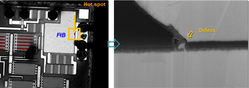
iST’s Exclusive Technique Efficiently Detects Hot Spots in GaN Chips
Four Key Applications of Nanoindentation and Scratch Testing for Advanced Packaging
Crystal Structures in Materials: The Key to Unbeatable Semiconductor Advanced Packaging
How to Identify & Analyze Ga2O3?
Among four major sectioning methodologies, which one is best for your sample?
Why is the 3rd Generation WBG Getting So Hot Nowadays?
Pinpoint Leakage Current Point of MIM Capacitor in Five Steps
Ideal cross section analysis tool for structural inspection of sizes greater than 100um
How Can iST Help You?
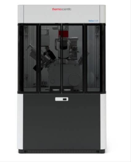
At iST, our Dual Beam FIB with Thermo Fisher Scientific Helios 5 has ultra-high resolution ion and electron beams for nanoscale positioning and observation of fine structures. An ion beam current reaches up to 65nA for fast cutting speed and lowered data access time.
Our Dual Beam FIB runs 24/7 across three shifts to provide customers with fast, high-quality services. Its Dual Beam FIB's high e-beam resolution detects voids and gate oxide sizes up to 3nm, and its vast area EDS detector allows contemporaneous cutting, shooting, and analyzing. We specialize in semiconductor component failure analysis, manufacturing line anomaly analysis, and nanoscale structure development for full analytical support. Contact our team of experts to learn more!

The Superiority of iST
Case Sharing
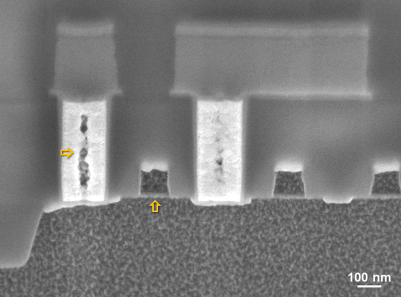
The H660 features excellent E-beam resolution for void and gate oxide of sizes up to 3nm (blue arrow marked) is identified clearly.
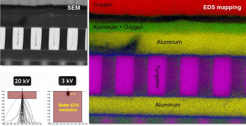
The large area (up to 150mm2) EDS detector comes with excellent space resolution for advanced application of "concurrent cutting, shooting, and analyzing".
Run entire EFA > PFA > FIB cross-sectioning processes by a professional failure analysis team.
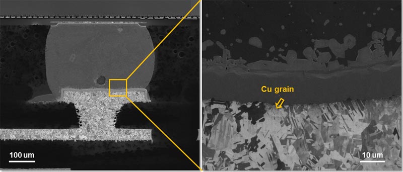
Get large area images of copper grains quickly with a special sample preparation approach (grinding + Ion milling).
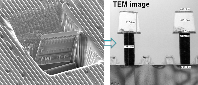
Prepare TEM sample up to 15nm thin.
- Failure analysis of semiconductor components (14 nm achievable)
- Anomaly Analysis of semiconductor production lines
- Epitaxy and structural analysis of thin films
- Voltage contrast test
- TEM specimen preparation
- Nanoscale structure preparation
Thermo Fisher Scientific Helios 5
- Maximum Size Of Sample:150mm
- 150mm2 SDD EDS Detector For Instant EDS Analysis.
- Equipped with high speed EBSD detector, the crystal information along with elemental analysis could be acquired simultaneously.
- For Observation Areas With A Width Greater Than 100um Or A Depth Of 50um Theis Recommended For Its Faster Cutting Speed.
| E-beam | I-beam | |
|---|---|---|
| Resolution | 0.6 nm at 15 kV 1.2 nm at 1 kV | 4 nm at 30 kV |
| Accelerate Voltage | 350 V - 30 kV | 500 V – 30 kV |
| Probe current | 0.8 pA – 100 nA | 1.1 pA – 65 nA |
Contact Window | Dr. Lin/Weijui | Tel:+886-3-5799909#6166 | Email:web_ma@istgroup.com