Issued Date:2023/5/16 EBSD
Issued By:iST
When Moore’s Law reaches its limit, advanced packaging has become the successor, but can it be successfully developed?
One of the keys lies in the crystal structure of the materials.
How to master the crystal structure code? It depends on the advanced analytical tool – EBSDEBSD

With the development of advanced processes, the size of chips has reached the physical limit of about 1 nm, and Moore’s Law is coming to an end. Advanced packaging technology has become the next key development direction, especially heterogeneous integration packaging technology with high chip integration capability, which has become one of the important technologies beyond Moore’s Law.
Recently, various countries have been expanding their capabilities in advanced chip packaging, including Korean companies investing heavily in order to overtake their competitors in advanced packaging technologies such as CoWos (Chip on Wafer on Substrate) and InFO/InFO-PoP (Integrated Fan-out / Integrated Fan-out-package-on-package).
At the same time, ChatGPT has also driven the demand for high-end artificial intelligence (AI) chip packaging. Major Chinese semiconductor packaging and testing companies are striving to enhance their High-Performance Computing (HPC) capabilities through advanced packaging technologies such as heterogeneous integration. Major Taiwanese semiconductor packaging and testing companies have already laid out their strategies in technologies such as FC-MCM (Flip-Chip-Multi-Chip-Module), FOCoS (Fan-Out Chip on Substrate), and VIPack (Vertical Integrated Package), and are vying for the HPC and AI packaging markets.
However, advanced packaging technologies for heterogeneous integration also face many reliability challenges and require early verification and analysis to ensure R&D quality. In past iST classrooms, we discussed issues such as the stress of advanced packaging material bonding, abnormal solder joints, and chip warpage (Further reading: Key to heterogeneous integration: Materials Bonding Stress;Finding advanced packaging joint defects after failing the board level reliability test;Two Obstacles, Challenges and Solutions for Advanced Packaging in Automotive Reliability)。
This time, we will focus on the “Advanced Packaging Material Characteristics” aspect to explore how crystal structure, defects, and strain affect the performance and reliability of advanced packaging components. How can we use existing tools to understand the characteristics of these advanced packaging materials? In this session of iST classroom, we will introduce the advanced analysis tool of crystal structure – EBSD, with three practical case studies.
EBSD
EBSD
What is EBSD?
We know that all materials are composed of atoms, which can be arranged into different crystal structures, and these structures determine the characteristics of the materials.
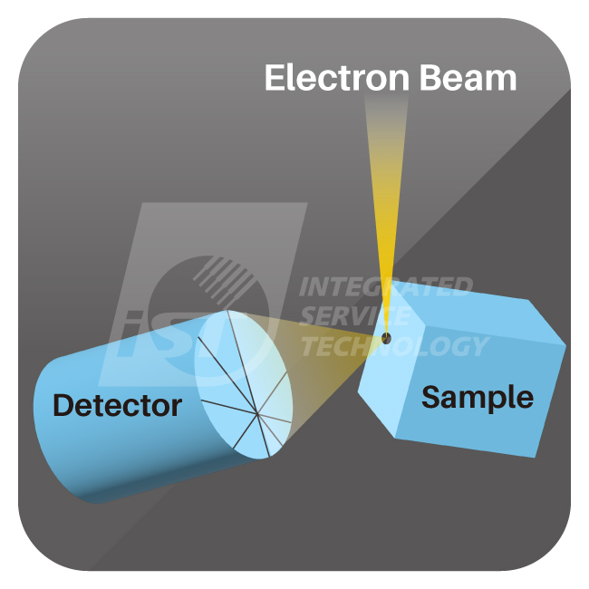
To analyze crystal structures, we rely on a powerful tool called EBSD (Electron Backscatter Diffraction). EBSD is a technique used to study the microstructure of materials, allowing researchers to analyze the crystal structure, grain boundaries, and hetero-material interfaces like using a magnifying glass but with greater precision and detail. This helps customers optimize material selection and process improvement.
EBSD technology has a wide range of applications in fields such as metals, ceramics, materials science, engineering, and electronics, especially in the semiconductor industry. By studying crystal structures, defects, and strain, EBSD can significantly improve the performance and reliability of semiconductor devices.
So how can EBSD be used? Here are three case studies from the iST Material Analysis Laboratory.
Case 1: Inferring the Anti-electromigration Ability of Copper Pillars from Grain Size and Structural Strength
Copper Pillar is a packaging technology widely used for the interconnection between semiconductor chips and packaging substrates, such as 3D IC packaging and FCBGA (Flip Chip Ball Grid Array) packaging. This technology uses small copper pillars instead of traditional wires to increase connection density and reliability, and achieve higher I/O (Input/output) density and performance.
EBSD analysis technique can provide qualitative analysis of the copper pillar’s crystal structure, including grain size, lattice orientation, and grain boundary angle. This data can be used to infer the anti-electromigration ability of the copper pillar.
1. Grain size: The smaller the grain size, the higher the density of grain boundaries, and the greater the hindrance to electron motion, resulting in better anti-electromigration ability.
2. Lattice orientation: Copper pillars with <111> crystal orientation have better anti-electromigration ability than those with <100> crystal orientation. This is because in <111> crystal orientation copper pillars, the area of grain boundaries is smaller, and electron motion is easier, resulting in better electron migration ability in this structure.
3. Grain boundary angle: When the grain boundary angle is smaller, the stress at the grain boundary is also smaller and the grain boundary is more stable. Therefore, it can be expected that copper pillars with smaller grain boundary angles will have better resistance to electromigration.
According to Figure 1, the proportion of grain boundaries with angles greater than 10 degrees is 94%, indicating that there is a larger difference in grain orientation, which may be unfavorable for electrical migration resistance. Figure 2 shows the statistical results of the copper pillar grain size, with an average particle size of 1.6um. Further comparison and analysis of the particle size and orientation data are needed. However, combining the results of both figures suggests that the copper pillar may not have good resistance to electromigration. The iST Material Analysis Laboratory suggests that researchers can further use high-temperature and high-humidity (HTH) and constant voltage (HVM) analysis to test its resistance to electromigration based on such results.
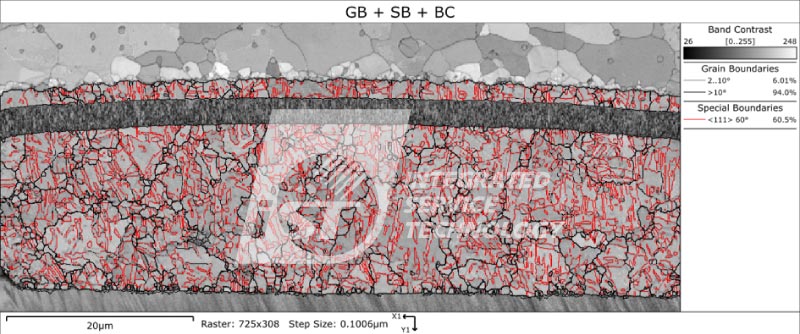
Figure 1: Distribution of grain boundaries in copper pillars, including high-angle boundaries (black), low-angle boundaries (light gray), and twin boundaries (red).
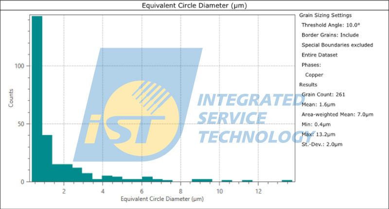
Figure 2: Statistical distribution of grain size.
Case 2: Analyzing the Intermetallic Compound to Confirm the Soldering Quality of Copper Pillars
In the solder joints of copper pillars, copper and tin complete the soldering process after eutectic reaction, and the Intermetallic Compound (IMC) at the interface is the key to copper-tin bonding. In a good soldering process, copper and tin will form a higher surface energy ball-shaped crystal (Cu6Sn5).
However, as the reflow temperature increases or the usage time lengthens, the interface in the joint will form degraded columnar crystals (Cu3Sn), which will reduce the strength and reliability of the joint. Therefore, the iST Material Analysis Laboratory recommends observing the distribution of the intermetallic compound at the copper-tin interface to compare the strength of the joint and thus confirm the soldering quality.
As shown in Figure 3, the phases of the copper-tin intermetallic compound are peach-colored Cu6Sn5 and sky blue Cu3Sn. The distribution and proportion of the phases can serve as a reference for evaluating the mechanical properties.
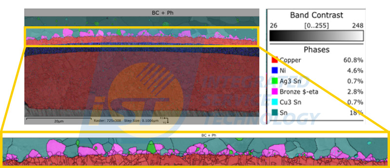
Figure 3: Phase distribution and their proportions of copper pillar (including copper-tin intermetallic compound).
Case Three: Observing Mechanical Strength and Anti-Electromigration Properties of Copper-Copper Bonding Interface
With advances in process technology, shrinking chip sizes, increasing computing power, and the growing number of connector joints, traditional high-density solder joints have reached their limits. Micro-solder joints not only have insufficient structural strength but also have inadequate heat dissipation and anti-electromigration capabilities to meet demand. Therefore, copper-copper bonding has gradually become a popular technology for advanced packaging.
In the method of copper-copper bonding, the twin boundaries of nanocrystalline copper can increase mechanical strength and reduce the risk of electromigration, and have good conductivity. Because copper atoms have the highest density on the (111) plane, this plane has thousands of times the diffusion rate of other planes. This method can be quickly joined at lower temperatures or shorter times, thereby avoiding the impact of high-temperature heat on heterogeneous integration and improving yield. By using EBSD to analyze its grain orientation information, we can grasp the mechanical strength and electromigration risk of the product in advance.
As shown in Figures 4 and 5, even with low-temperature rapid bonding, the two copper pad layers have not diffused with each other. Although their preferred orientation is (111) and has better anti-electromigration capabilities, the interface can still be observed significantly, indicating weaker mechanical strength and the risk of interface separation. Figures 6 and 7 show that although the interface between the copper pad layers disappears, indicating better mechanical strength, the preferred orientation results show that it may not have excellent anti-electromigration properties.
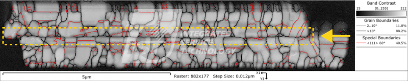
Figure 4: Grain boundary distribution of copper-copper bonding at 150°C, the dashed circle highlights the copper-copper bonding interface.
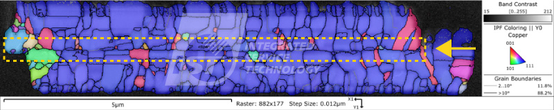
Figure 5: Orientation map of copper-copper bonding at 150°C, the dashed circle highlights the copper-copper bonding interface.
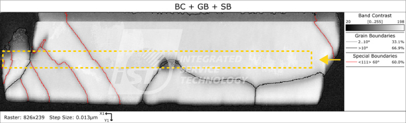
Figure 6: Grain boundary distribution of copper-copper bonding at 350°C, the dashed circle highlights the copper-copper bonding interface.
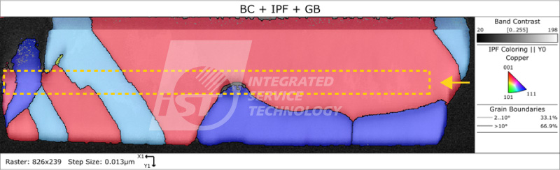
Figure 7: Orientation map of copper-copper bonding at 350°C, the dashed circle highlights the copper-copper bonding interface.
In this iST classroom, we introduced three EBSD case studies related to material characteristics in advanced packaging. Other hot topics related to advanced packaging include: How to choose the next type of semiconductor materials? How to measure and analyze the thermal characteristics of heterogeneous packaging materials? Please continue to stay tuned to iST’s sharing for further information on these topics.
iST Material Analysis Laboratory has been working in the semiconductor and advanced packaging fields for a long time and has accumulated considerable experience and successful cases. If you have any related needs or want to further understand the relevant knowledge, please feel free to contact Mr. Weijui Lin at +886-3-579-9909 ext. 6166 or email at
web_ma@istgroup.com;marketing_tw@istgroup.com。
References:
1. Yu-Jin Li , King-Ning Tu and Chih Chen . Tensile Properties of -Oriented Nanotwinned Cu with Different Columnar Grain Structures. Materials 2020, 13, 1310.
2. Chien-Min Liu , Han-Wen Lin , Yi-Sa Huang , Yi-Cheng Chu , Chih Chen , Dian-Rong Lyu , Kuan-Neng Chen & King-Ning Tu. Low-temperature direct copper-to-copper bonding enabled by creep on (111) surfaces of nanotwinned Cu. Sci. Rep. 5, 9734; doi: 10.1038/srep09734 (2015).
3. Chen, Y., Tong, Y., Lu, Y., Chen, Y., Liu, X., Zhang, Y., … & Lu, J. (2020). Enhanced strength and ductility in a high-entropy alloy via ordered oxygen complexes. Nature Materials, 19(11), 1351-1358. doi: 10.1038/s41563-019-0579-x.
4. Kwon, O., Park, J., & Kim, H. (2013). Enhanced strength and thermal stability of nanocrystalline Cu and Cu alloy wires with bimodal grain size distribution. Acta Materialia, 61(1), 71-80. doi: 10.1016/j.actamat.2012.09.003.
5. Xu, J., Zhang, X., Zhang, J., & Liu, Y. (2010). Improved electromigration resistance in nanocrystalline copper interconnects with a bimodal grain size distribution. Microelectronics Reliability, 50(3), 391-396. doi:10.1016/j.microrel.2009.10.004.