Issued Date: 2016/10/26
Issued By: iST
What else can you do to identify peeling in a product’s structure when cross sectioning by conventional grinding is out of choice?
Is there any time saving, quick, and full structure-viewable tools for large area analysis of PCB, 3D IC, or through-silicon via (TSV) or solder bumps?
Questions like these two have been arriving at iST often lately. In general, Dual-Beam FIB is ideal for cross section analysis of local and small areas which enables fast structural diagram generation with its shooting-while-cutting feature.
This is not the case for large range structural observation (section size greater than 100um or depth greater than 50um) over PCB, TSV, 3D devices, and solder bumps. The limited etching speed and scope of Dual-Beam FIB (DB FIB) is especially so when both fixed-point analysis and concurrent image generation are needed at the same time.
To overcome these drawbacks, we recommend Plasma FIB (PFIB) to replace DB FIB. The former not only features the same shooting-while-cutting capacity possessed by DB FIB but also enables large scope observation to present the whole structure in the target area at etching speeds 20 folds faster than traditional DB FIB. This improves analysis speed effectively.
| PFIB | DB FIB | |
|---|---|---|
| Ion source | Xe ion plasma Ga ions tends to attach to the sample surface Use of Xe reduces sample contamination by Ga ions | Ga+ ion |
| Etching speed (Probe current) | 1.3μA Capable of running over large areas at fast speed | 65nA |
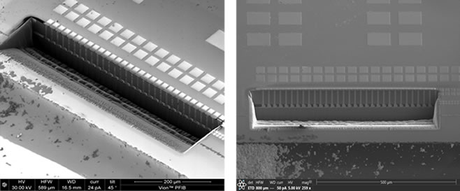
- PFIB can be applied in the following fields:
- Large range structural observation (100μm or more) including 3D, TSV structures, solder bumps, and packaging products;
- Delayer application for advanced processing of 16nm or narrower.
See the cases below for some examples of the use of PFIB.
Case1:Solder Bumps
Instead of local observation of the peeling of solder bumps by conventional methods, the PFIB tool cross sections solder bumps for overall inspection. With a width of cutting point up to 500μm in 2 hours, it far outperforms its older counterpart’s long working hours (10 or more) and limits of local area observing.
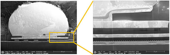
Full solder bump image
Local area observation available
Case 2: TSV structure observation
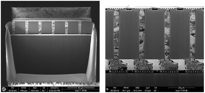
PFIB features good etching efficiency in a large range for fast and complete presentation of multiple TSV structures.
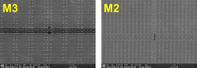
Case 3: IC delayer
Observing micro structures by advanced process of 16nm or narrower by conventional grinding suffers as the structure is too thin to grind properly. That is, grinding off 2 layers in one treatment or uneven structures after grinding. This is exactly not the case with PFIB as it can grind off structure of large size and layer by layer with plasma etching.
We at iST have been striving to share inspection and verification experiences with you. In case you have a sample structure requiring observation, determination and inspection, or just want to know more about this technique, call Mr. Lin at 03-579-9909 Ext 6166 or Mr. Li at Ext 6174 or send an email to web_ma@istgroup.com.