Issued Date: 2018/8/29
Issued By: iST
Always end up with improper analysis methods and instruments when identifying IC defects?
Addressing virtually invisible process issues and nano-grade surface contamination, what is the best approach to analysis?
The most frequent problem raised by customers in iST’s more than two decades of verification analysis history is: “When addressing the failures we encountered, which tools can be used to identify our contamination defects?”
Contamination defects come in two types: visible and invisible. Both are killers in the IC manufacturing process and causes of product failure or future errors. Visible contamination is easier to catch: magnify suspects with optical or electron microscopy to hundreds of thousands times magnification and they have nowhere to hide. This is not the case with virtually invisible and intangible contamination: where, and what, are the suspects?
What we are going to share with you in the iST Tech Classroom this month is how to select the right surface analysis tools to identify these visible/invisible contamination defects.
It may be required to identify nano-grade small and thin foreign matters at early R&D stage to determine the steps in production and manufacturing leading to them. It’s quite possible to encounter electrical anomalies, high resistance (or open circuit), short circuit or leakage due to oxidation or contamination by RDL/UBM process at the final packaging, testing, and assembling stage. All these invisible defects can be found only by surface analysis tools.
Here are the six major criteria for determining surface contamination:
(I) Is further composition analysis required after contamination pattern measuring and imaging? Try AFM first.
iST found that most of our customers tend to identify process contamination defects with Scanning Electron Microscopes (SEM), measuring and imaging contamination particles, and getting composition data with Energy Dispersive X-ray Spectrometers (EDS) mounted on SEMs. Is this valid for measuring surface contamination defects in samples?
No, it’s wrong for it!
SEM based surface analysis can see the clear image patterns of surface contamination only after samples are made conductive by metal (Au or Pt) plating. There is a severe side effect: it hampers regular contamination composition ingredient analysis in the future, as the Au plated surface gives signals of Au rather than the actual composition of regular contamination.
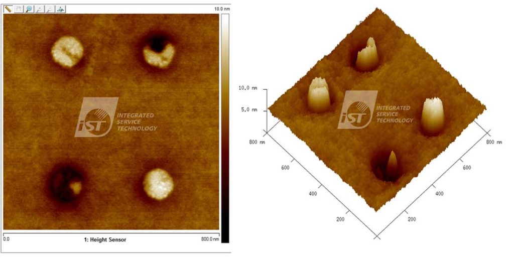
Atomic Force Microscope (AFM) outpaces SEM due to its atom rather than electron-based imaging. AFM analysis can not only directly scan the contamination surface signal and acquire clear 3D profiling, but also enable later contamination composition analysis without interference as the sample can go without metal plating for conduction.
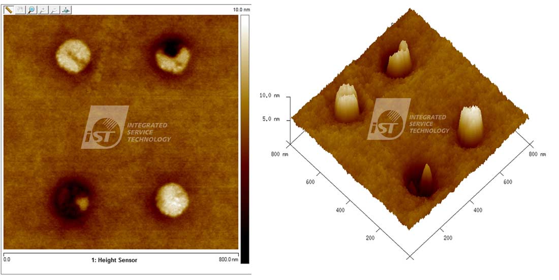
2D and 3D AFM images of contamination on Si wafer surface at 0.1um scale
(II) Before analyzing contaminated compositions, determine their scale first.
iST found that most customers are likely to rely on fast composition analysis using SEM EDS for identifying process contamination defects. The problem with EDS is that it measures from the bottom of the sample with X-ray reflection signals which give the “bottom” substrate signal of the sample rather than the contamination on its surface. That is, EDS is not a good device for surface contamination analysis.
- For contamination of scales above 10um, choose XPS/ ESCA
XPS/ESCA instruments are recommended for qualitative and semi-quantitative analysis - Otherwise, choose AES
Auger Electron Spectroscopy (AES) are recommended here.
Both instruments feature an upper limit of concentration detection around 0.1atom% and are applicable to elements of atomic number 3 (Li) in the periodic table.

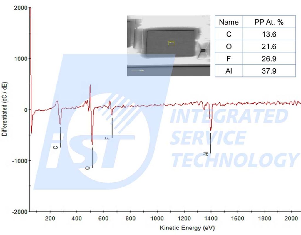
AES analysis over IC contamination by F ingredients from the aluminum pad
- For contamination of scales above 10um, choose XPS/ ESCA
(III) Choose XPS/ ESCA in case chemical state/bonding of contamination is required.
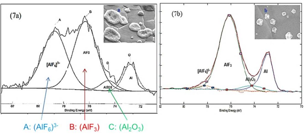
Explore the “chemical state/bonding” of the contamination using XPS/ ESCA to drill down qualitative chemical elements by surveying the bonding state of compositions and determining their chemical differences. Remember: contamination scale must be 10um or larger.
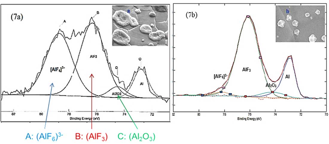
XPS based chemical state analysis over residuals of different morphology by aluminum pad process (picture courtesy of: Y. Hua et al., IPFA 2014)
(IV) Is identifying contamination with organic substances required?
- In case of contaminations of 1um or thicker and 30um or bigger, choose FTIR
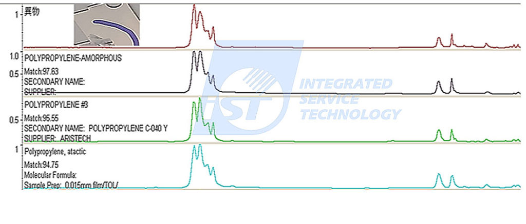
Employ Fourier-transform infrared spectroscopy (FTIR) for organic analysis when C, O, N, and similar elements are found by qualitative analysis. Working with iST’s huge internal spectrum database, the FTIR may survey foreign matter of 1um or thicker and 30um or bigger. - In case of contaminations of 1um or thicker and of sizes below 30um, choose Raman
Use a Raman spectrometer to identify foreign matter of the aforementioned sizes. iST’s Raman spectrum database may be added with substances employed by the manufacturing process before proceeding with foreign matter analysis and identification.
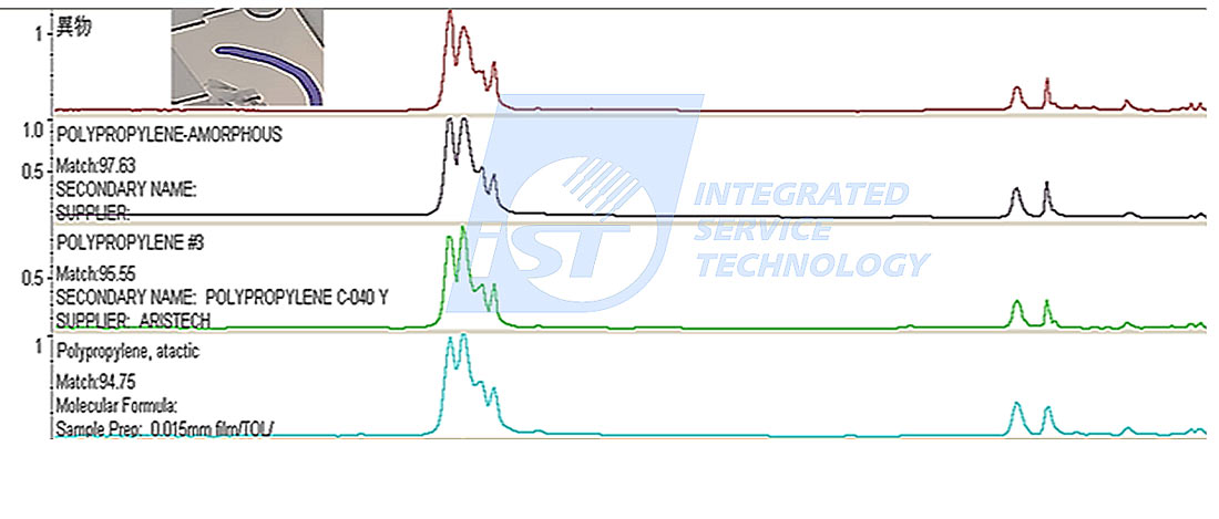
Organic contamination on metallic racks surveyed and identified by FTIR: PP polypropylene
- In case of contaminations of 1um or thicker and 30um or bigger, choose FTIR
(V) Dimension of invisible super-thin contaminations bigger than or less than 10um
- For contaminations of 10um or wider, choose XPS/ ESCA
For invisible foreign matter with contaminations tens of nm thick and sample target measurement area widths of 10um or larger, choose XPS/ESCA. - For contaminations of 10um or narrower, choose AES
Choose AES for sample target measurement area widths of 10um or narrower. - Choose SIMS for identified organic contamination
Organic contamination shall be surveyed by Static Secondary Ion Mass Spectroscopy (Static SIMS). The latter are most likely in the form of TOF-SIMS, and applicable to elements of atomic number 1 (H) in the periodic table and target measurement areas larger than 100um.
- For contaminations of 10um or wider, choose XPS/ ESCA
(VI) Choose SIMS for quantitative contamination analysis
Standard samples of known concentrations employ quantitative analysis to calculate concentrations of unknown contamination samples. Dynamic SIMS is ideal for quantitative analysis of trace contamination elements in materials including Si, InP or GaAs bases due to its characteristics of high ion yield and extremely low detection limit. With concentration detection limits at ranges of ppma-ppba, the SIMS quantitative analysis is applicable to target measurement areas above 100um and thicknesses above 100nm.
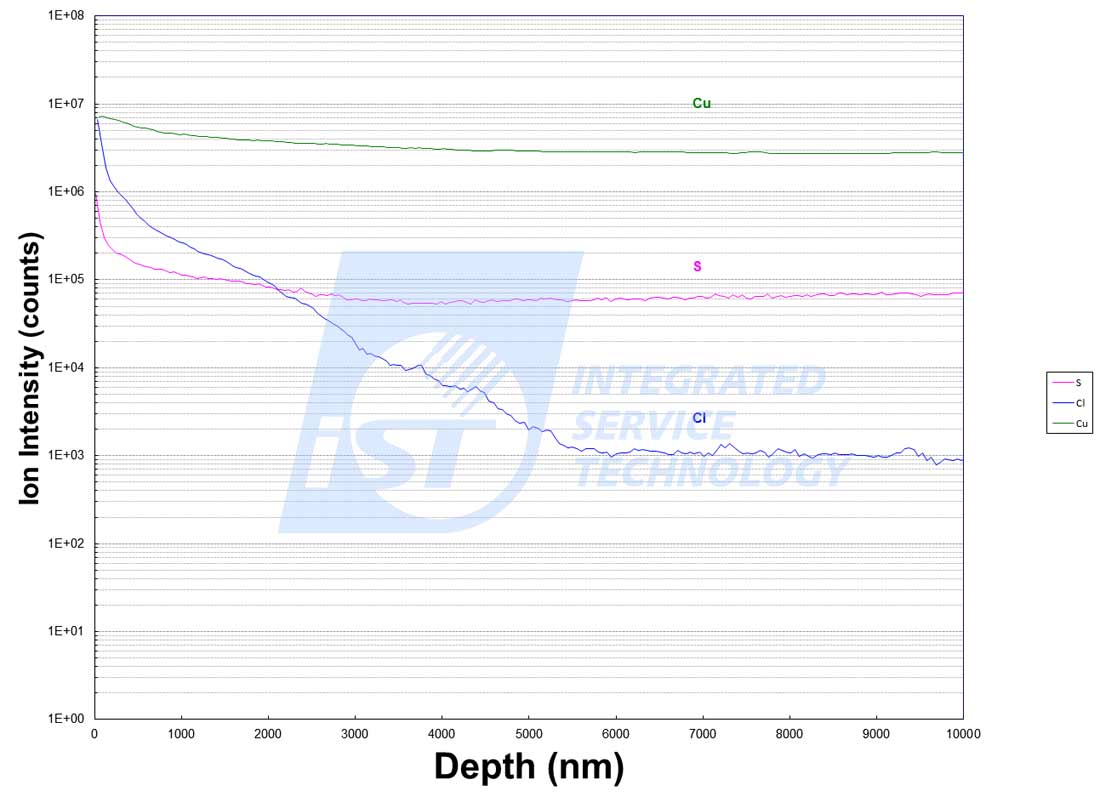
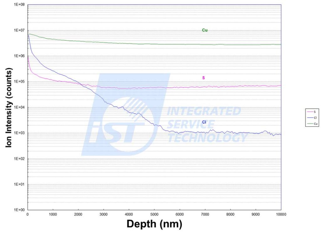
SIMS analysis over Cl elements of invisible surface contamination
This article is aimed to share our detection and verification experiences with honorable clients like you. To know more about estimating depth and dimension of contamination and desired concentration level and analysis flow chart, just ring Mr. Johnson at +886-3-579-9909 Ext. 6613 or email him at sa_tw@istgroup.com and marketing_tw@istgroup.com. You’ll get two copies of sophisticated and comprehensive diagram which may help you to choose valid analysis instrument on the fly.