Issued Date:2021/3/9Surface Roughness
Issued By:iST
Surface roughness is critical to the adhesiveness of coating and varies with the product and process.
Measuring roughness plays a key role in process improvement. The challenge is: which analysis tools can meet this demand?
Surface Roughness
Most of us know that the bottom of hiking and jogging shoes or tire surface of off-road vehicles would make use of larger particles to add friction. This is the opposite case for surface of cleaning appliances or coats as they are designed to have weaker surface adhesion to prevent liquid from attaching to them once being washed or spilled on.
All these are surface roughness-relevant. The same goes true with the surface of electronic products and wafer processing as surface roughness is critical in the processes including cleanliness after cleaning, adhesiveness of coating and directionality of etching.
Requirements on the roughness may differ significantly among individual products, processes or samples. Take as an example: The average surface roughness of a wafer or glass is kept up to 1nm and goes a little higher after micro etching and cleaning for better adhesiveness in the later coating steps.
Thanks to repeated operations and interactive effects imposed by etching, coating and mechanical stress, wafer carriers of process equipment may suffer variance in roughness up to tens or hundreds of nanometers. To measure surface roughness in such a wide range of scope and precision requirements cannot rely on a single instrument let alone the dimension of samples may mandate different instruments from the beginning.
Now, the question is which measurement tools should be chosen out of a spectrum of products? This iST Tech Classroom “Determine exact surface roughness with the help of three tools” will help you answer it.
Difference of vertical height between real and ideal surface, see Figure 1. Both AA Ra (Arithmetic Average Roughness) and RMS Ra (Root Mean Square Roughness) defined by ISO and ANSI can be used to calculate value of and changes in the roughness of samples to guide process improvement.
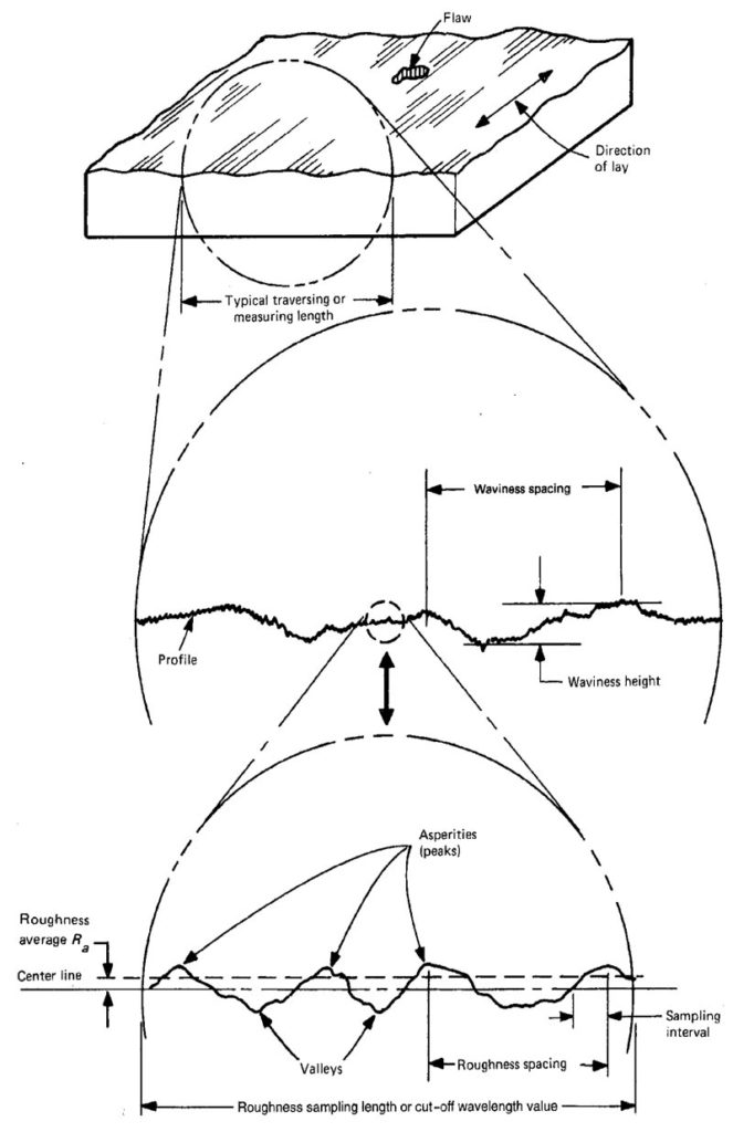
Figure 1. source: ANSI/ASME B46.1, ASME, New York
1. Measure Roughness with Three Advanced Tools
Surface Analysis
Surface roughness is used to be measured by contact scanning the surface with a tungsten steel probe (Figure 2). This is OK with products of harder solid substance or only suitable for simple height difference measurement as the probe may suffer greater radius of curvature and may leave the surface with scratches and deformation (e.g., Surface profiler/Alpha-Stepper). It also fails with measuring ICs of photoresist substances and softer polymers.
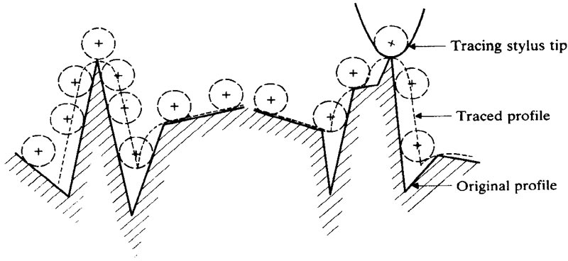
Figure 2: Real surface profile may be subject to the radius of curvature of probes (source: Modern tribology handbook 2001 by CRC Press LLC)
The iST lab provides you with three analytical tools for surface roughness measurement: White Light Interference (WLI), Atomic Force Microscopy (AFM), X-Ray Reflectometry (XRR)
1. WLI for Samples of Larger Size and Opaque Materials
WLI Employs the theory of optical interference (Figure 3), i.e., spacing of constructive interference fringes equal to the fixed wave path difference, to calculate the height into a 3D topography based on surface profiling (Figure 4) which, in turn, is used to calculate surface roughness. WLI is ideal for samples of a larger size, up to 100um or even a couple of millimeters, as it relies on optical microscope for the measuring.Surface Analysis
WLI is most likely adopted for profiling the surface of opaque materials including metals, circuits, plastics rather than translucent ones (e.g., glass). Other analysis technology is required when the surface of the material under test cannot be applying metal plating for WLI measurement.
See Figure 5 for a metal surface after acid cleaning and its roughness (average greater than 1um) measured over a surface square of 300um.
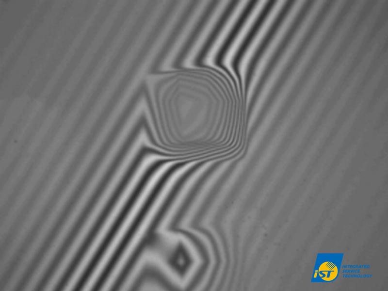
Figure 3: White light interference
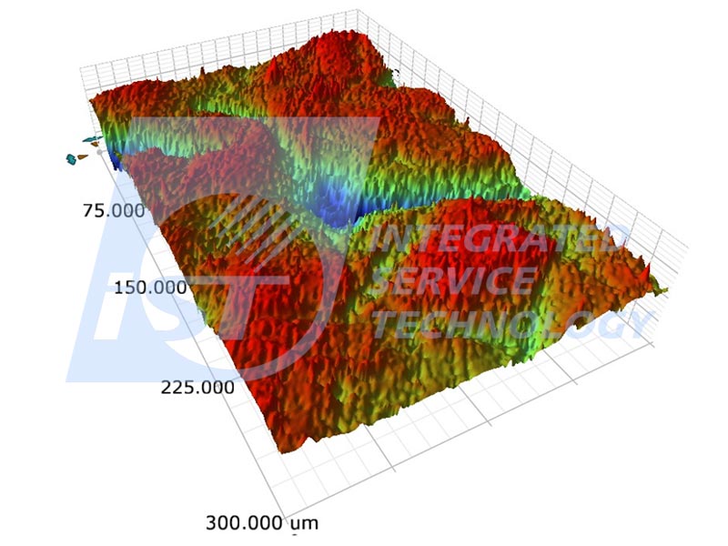
Figure 4: 3D profiling
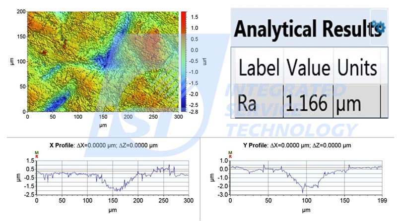
Figure 5: 2D/1D profiling and roughness analysis in the value of Ra
2. AFM for Samples of Wafer and Glass Materials
AFM employs nano-probes to profile samples of very flat surfaces or soft polymers (e.g., photoresist) for surface roughness measurement. It is widely adopted in micro analysis over an area of tens of microns on the surface of the wafer and glass pre- and post-cleaning, coating and etching.Surface Analysis
It is widely used in IC’s chemical mechanical polishing (CMP), redistribution layer (RDL) and under bump metallization (UBM) process now. Researches are focused on measuring and monitoring difference pre- and post-etching as any abnormal roughness is very likely to result in a loss of coated film and even reliability issues.
See Figure 6 for the profile of a 2um square surface on PI polymers with an average roughness at around 8nm. To compare its pre- and post-roughness a non-destructive measurement is required. The AFM device mandates not only the necessary measurement capabilities but also a sample jig of a size up to 12 inch to measure 12″ wafers.
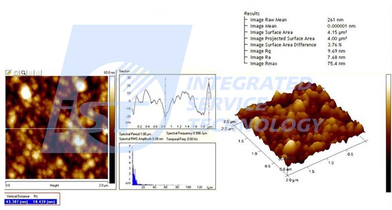
Figure 6: AFM profiling and roughness analysis in value of SAD%, Rq and Ra
3. XRR for Samples of Multi-Layer and Ultra-Thin Film
X-ray diffraction (XRD) device comes with XRR (X-ray Reflectivity) analysis function. The former is diffraction and the latter reflection-based. Measuring roughness by fitting a total reflection spectrum with analysis software, the XRR is ideal for ultra-thin film’s roughness measurement. For a film with a total thickness of up to 500nm, XRR is effective for roughness, thickness and electronic density measurement.
In case of multi-layer samples, the XRR outrun WLI and AFM by measuring not only roughness of the top layer but also the interface roughness in between films or film and substrate. In addition, XRR is not limited to crystal materials, that is, it is OK to measure the roughness of amorphous organic materials.
However, it is limited by an average roughness of the film surface as it relied on X-ray reflection and won’t work if greater than 5nm.Surface Analysis
Process of making semiconductors is employing increasingly more nano-thick films now. XRR can be easily used to non-destructively measure the roughness of a sample wafer coated by 7nm aluminum oxide film which an AFM microscope has no way of getting its thickness measurement.
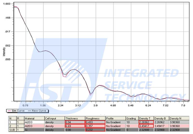
Figure 7: XRR fitting analysis for thickness, roughness, and density of Alumina film
2. Sum up Characteristics of Three Roughness Analysis Tools in One Table
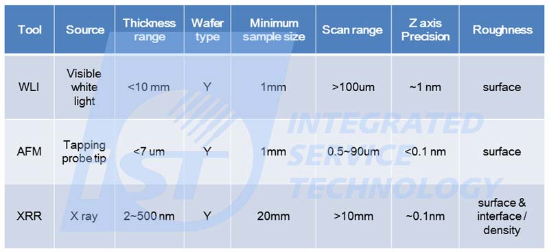
Samples tested by these three tools do not require a vacuum environment. That is, they can be analyzed directly and can go on with more tests as they are subject to no damages at all. See Table 1 for a summary of these three measurement equipment which is provided for you to select the best equipment to get effective analysis data based on the dimension of the samples to be tested and scope of roughness measurement required.
Table 1: Tools for surface roughness analysis
This article is intended to share our experiences with valued clients like you. Should there be any inquiry or if you would like to know more about the aforementioned techniques, just ring Mr. Chang at +886-3-579-9909 Ext. 6613 or email him at sa_tw@istgroup.com.