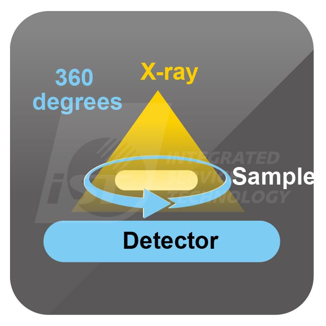
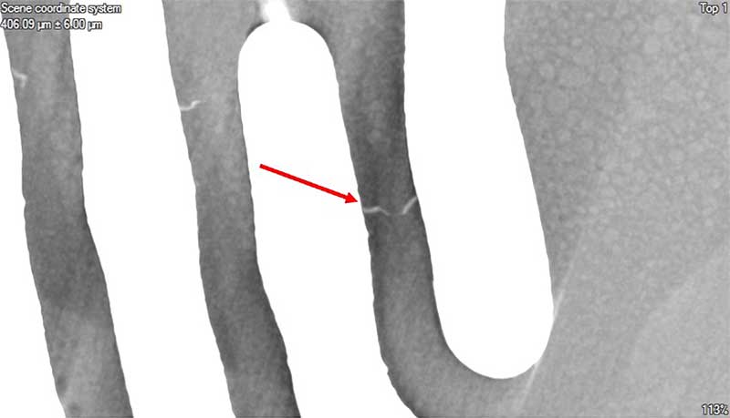
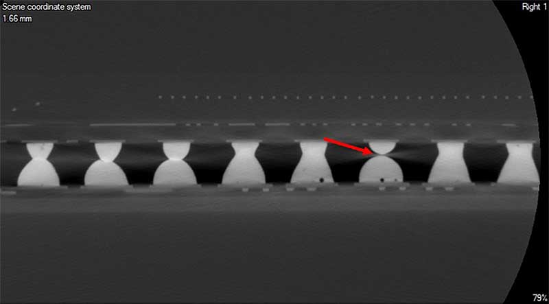
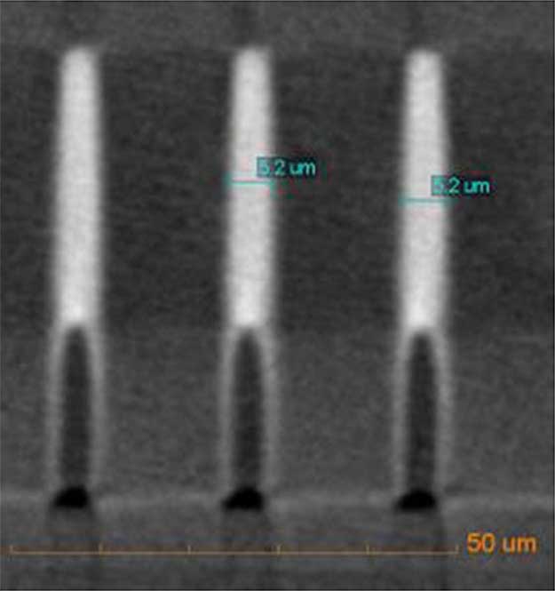
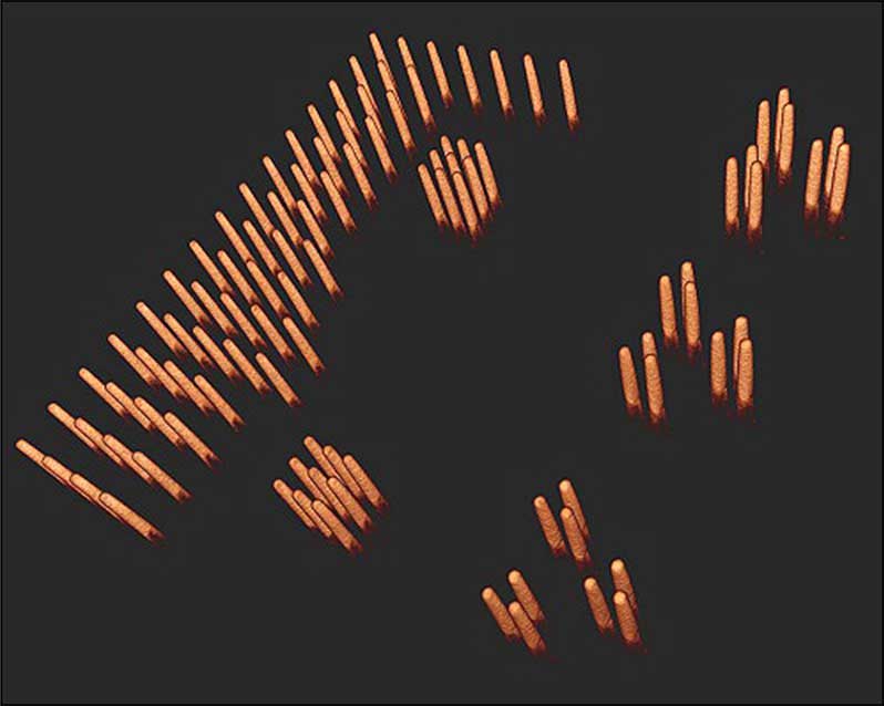
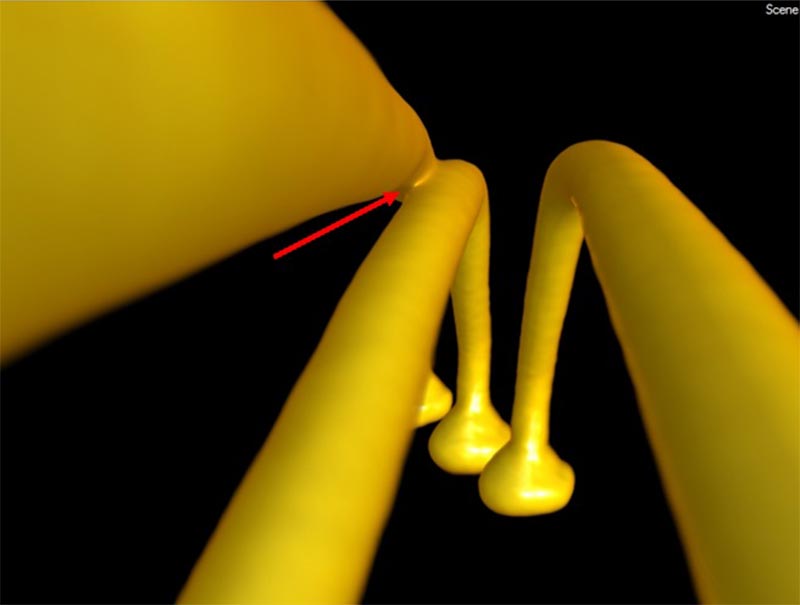
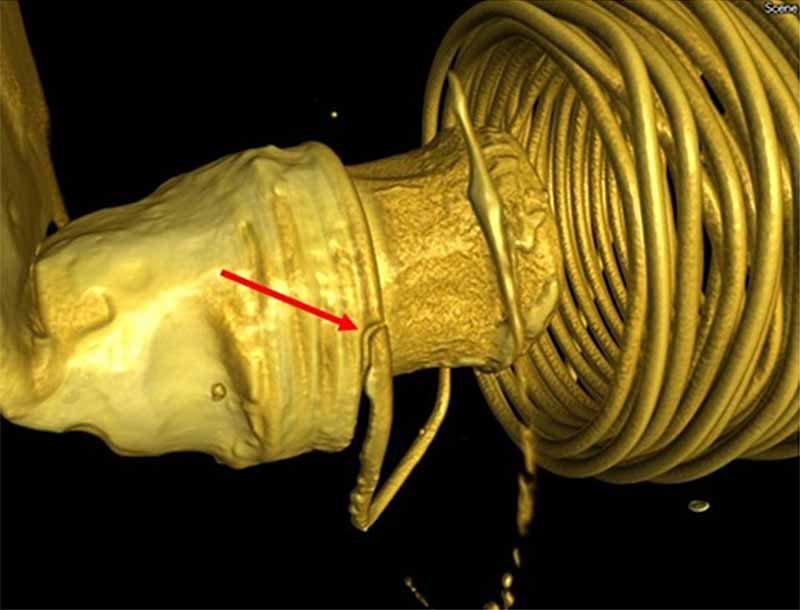
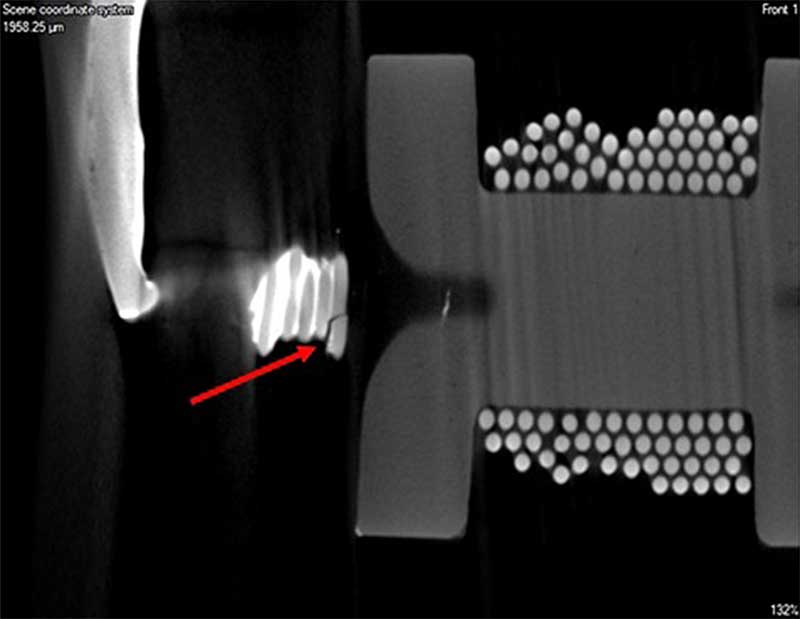
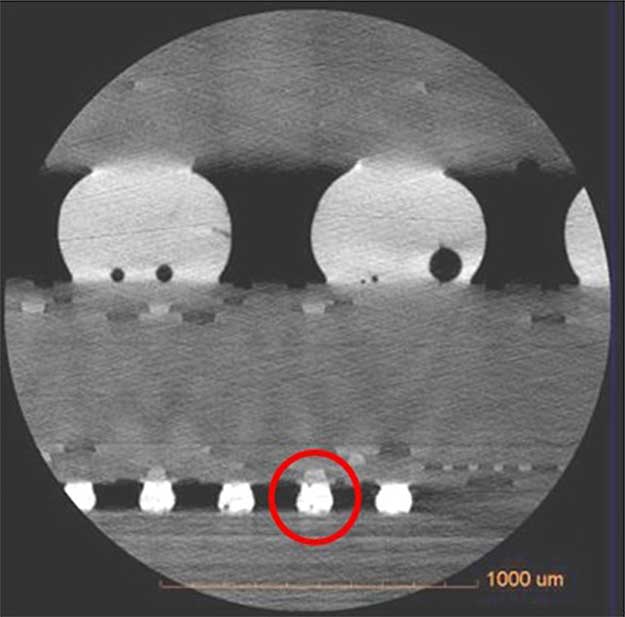
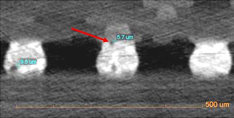
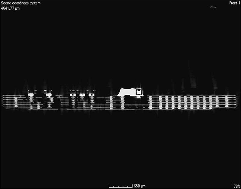
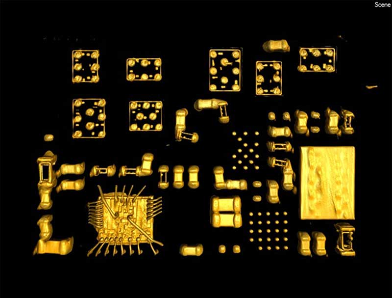
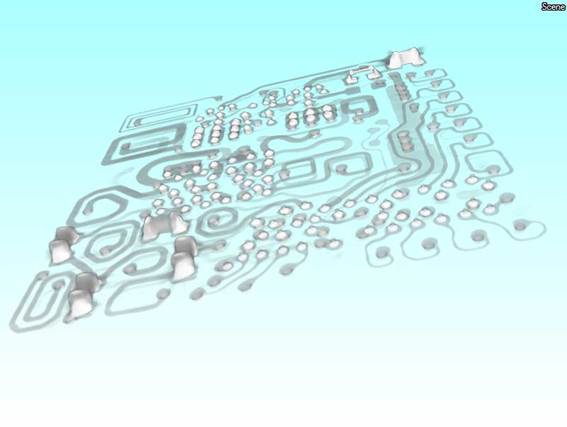
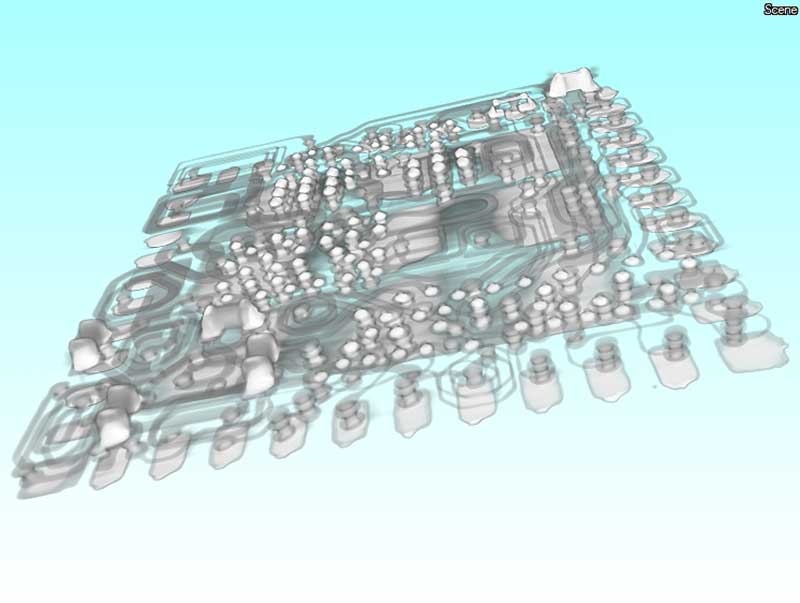
High Resolution 3D X-ray Microscope is a non-destructive method employed with an optical microscope to enhance the magnification, which uses 2D X-ray tomography to take sample images at all angles while turning the fixed sample 360 degrees. Physical images of the tested object are then constructed by computer operation.
The Superiority of iST
Case Sharing
- Defect inspection during IC packaging such as inspections of wire bonding, plastic cracks, bubbles in epoxy or plastic, etc.
- Potential process defects in PCBs and carrier boards, such as circuit miss-align or bridge and open circuit, quality inspection of plated via process, multi-layer PCB layout analysis.
- Defect inspection in all electronic products, including open circuit, short or abnormal connections.
- Solder ball integrity inspection of BGA and flip chip packages, including solder ball deformation, crack, cold soldering, short, and blow hole.
- Crack inspection of high-density plastics or cavity inspection of metals.
- Inspection and analysis of active and passive components.
- Structure inspection of various materials.
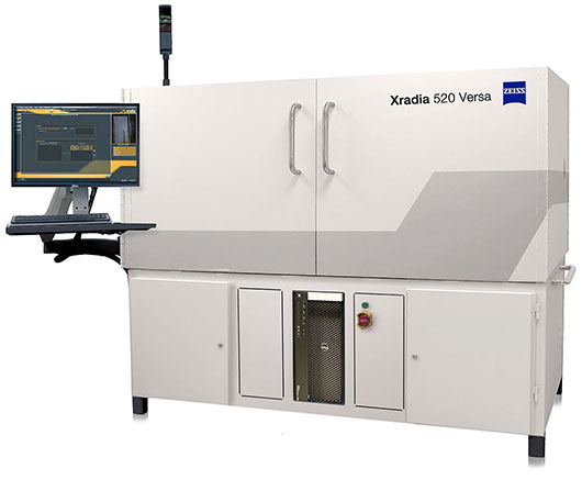
ZEISS Xradia 520 Versa
- In case the IC package contains low density material, the X-ray may penetrate the material and be unable to detect it.
- Sample size to be no more than 300mm. Maximum weight < 15 kg.
Contact Window | Mr. Chang/Hp | Tel:+886-3-5799909#6580 | Email:web_nde@istgroup.com

