Issued Date:2025/5/6X-ray TID
Issued By:iST
To precisely identify internal defects in ICs, non-destructive 3D X-ray inspection has become a critical technique in the semiconductor industry. However, ICs subjected to excessive radiation doses may suffer premature failures. As the application of semiconductors expands into AI, automotive, aerospace, and medical devices—domains that demand exceptionally high reliability—engineers must now confront the challenge of measuring and controlling parasitic radiation-induced effects.
X-ray TID
X-ray imaging is a non-destructive physical analysis technique that enables real-time, convenient diagnostics for failure analysis (FA) and process improvement. Under most standard operating conditions, it poses no electrical risk to components. However, under certain process or product-specific scenarios, electrical characteristics may be adversely affected.
Just as prolonged exposure to radiation in humans can lead to cellular mutation, DNA damage, and increased cancer risk, ICs can exhibit similar vulnerabilities. When ICs undergo repeated or excessive non-destructive evaluations—such as 2D X-ray or 3D X-ray imaging—the accumulated radiation dose, referred to as Total Ionizing Dose (TID), can alter transistor characteristics. These changes may include an increase in gate leakage current or gate oxide degradation, ultimately accelerating early-life failures., ultimately accelerating early-life failures.
As AI, automotive, and aerospace applications place increasingly stringent demands on long-term reliability, risks that were previously overlooked must now be addressed. In response to this, JEDEC released JESD22-B121 in November 2023. This standard defines a methodology for evaluating post-irradiation electrical behavior of ICs during manufacturing, inspection, and Surface Mount Technology (SMT) processes. It further introduces the concept of a TID limit—defined either as a failure limit or a supplier limit—to mitigate latent failure risks.
In this iST Tech Classroom article, we explore the radiation-induced failure modes in electronic components, identify critical test parameters, and explain how to interpret the final report of TID characterization. We also introduce iST’s proprietary Parasitic Radiation Dose Deposition Validation Platform, which enables engineers to proactively assess and prevent X-ray-induced degradation in ICs.
X-ray TID
X-ray TID
1. Radiation Dose Failure Mechanisms and Failure Modes
To evaluate changes in critical electrical parameters, engineers must first understand the failure mechanisms triggered by ionizing radiation—particularly the accumulation of trapped charge in dielectric layers. When ICs are exposed to X-ray radiation with cumulative effects, these trapped charges can shift internal parameters such as threshold voltage or leakage current, increasing the risk of functional degradation or early failure. Radiation assessment is thus a critical part of IC reliability engineering, allowing designers to quantify radiation tolerance and define safe operating margins.
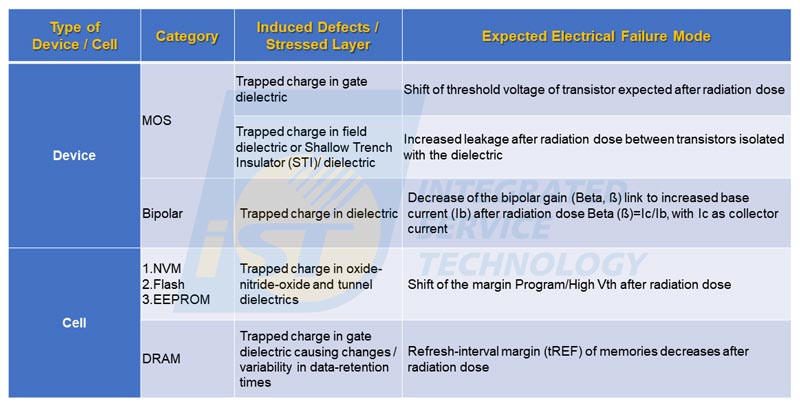
Different materials absorb radiation at different rates. When the device is exposed to an X-ray source with photon energy, a parasitic dose can be deposited through the energy absorbed by the device. This accumulation or Total Ionizing Dose (TID) may result in irreversible electrical degradation, as outlined in Table 1.
The induced failure mode is typically a drift in one or more electrical characteristics that causes the IC to malfunction. TID is considered to be a permanent effect on electronic devices even though some recovery may occur. Radiation damage is considered an intrinsic effect of the deposited parasitic dose. Table 1 show the most expected failure modes for major IC device or cell types.
2. X-ray System Settings and Variables
X-ray imaging techniques are widely used to inspect IC package structures, particularly for identifying hidden defects in internal layers. These methods complement optical inspection, which is more suited for detecting surface anomalies. In semiconductor applications, X-ray systems are also used during device shipment scans, solder joint inspections, and failure analysis of returned materials—all of which contribute to cumulative exposure. Therefore, the X-ray system employed for product inspection can be used to characterize the total ionizing dose (TID) that may affect device performance. Figure 1 shows a simplified schematic of an X-ray system.
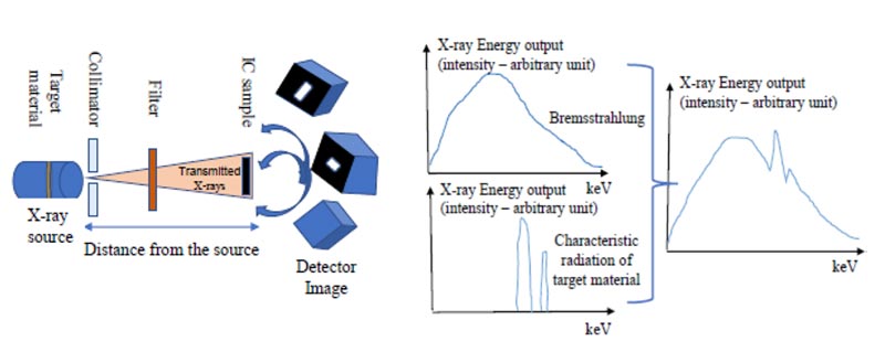
Figure 1: Simplified schematic of X-ray system(Source:JESD22-B121)
When a high-energy electron or ion beam strikes a metal target—commonly tungsten—X-ray photons are generated. These photons originate from two primary mechanisms:
- Bremsstrahlung Radiation:
Continuous-spectrum X-rays are emitted as incoming electrons decelerate due to the Coulomb field of atomic nuclei. - Characteristic Radiation: Discrete-energy X-rays are produced when incident electrons displace inner-shell electrons of the target atoms, resulting in electron transitions that emit photons at specific energies.
As X-rays penetrate and surround the sample, the detector captures both absorption and scattering signals from various materials, forming a radiographic image. The image contrast depends on the material’s X-ray absorption coefficient—regions with lower absorption appear brighter, while those with higher absorption appear darker.
The quality of the X-ray image and the radiation dose absorbed by the IC are both influenced by system parameters. For example, 2D X-ray imaging captures a single-angle projection with a relatively low dose but may suffer from occlusion in multi-layered structures. In contrast, 3D X-ray imaging reconstructs volumetric images through multi-angle scanning, improving structural visibility but significantly increasing the total ionizing dose (TID).
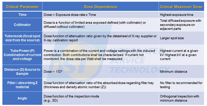
To evaluate radiation-induced degradation in functional ICs, Table 2 defines the critical maximum dose under different system configurations. To ensure the TID limit is not exceeded during inspection, engineers should optimize system parameters—such as reducing tube voltage, minimizing exposure time, and selecting appropriate scan modes. Additionally, the X-ray system should be capable of delivering a stable and uniform dose rate at the chosen operating voltage and power settings, to avoid variability in cumulative exposure.- Bremsstrahlung Radiation:
3. X-ray Radiation Dosimetry
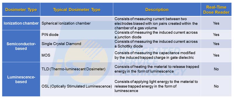
To accurately characterize the radiation dose-rate within the material of interest, the test setup must include an X-ray inspection system capable of generating a stable and consistent radiation output, along with a calibrated dosimeter to measure the absorbed dose-rate precisely. The X-ray system should be configured to simulate typical inspection conditions based on key operational parameters. Table 3 shows the types of dosimeters available for TID measurement.
Ionization chambers and semiconductor-based dosimeters are classified as active devices, capable of measuring the electrical current generated by incident radiation in real time. This allows for immediate dose-rate readout during X-ray exposure.
In contrast, luminescence-based dosimeters—such as thermoluminescent dosimeters (TLDs) and optically stimulated luminescence dosimeters (OSLDs)—are passive devices. These store radiation information internally and require post-exposure readout via heating or optical stimulation. As a result, dose data cannot be accessed immediately after irradiation.
When using luminescence-based dosimeters, it is recommended to store them at room temperature under standard environmental conditions to prevent degradation from heat or UV exposure. Extended storage and transportation time should also be minimized, as environmental factors can affect dose accuracy.
If environmental conditions are known to impact dosimeter response, correction factors must be applied to the measurement results. Additionally, secondary or reference dosimeters may be employed to account for stray or unintended exposure and subtract it from the primary dosimeter’s reading used for system calibration.
Calibration of readout systems across the expected energy range is also essential. Industry standards such as ISO/ASTM 51956 (e.g., “Practice for Use of Thermoluminescence Dosimetry (TLD) Systems for Radiation Processing”) provide guidance for accurate measurement and system setup.
4. Test Procedure for TID Characterization
Figure 2 illustrates the schematic flow for Total Ionizing Dose (TID) testing under X-ray exposure. Two characterization modes can be implemented during this procedure, and both should be clearly documented in the summary report:
- Supplier Limit Characterization
This mode evaluates the maximum dose a device can tolerate during standard inspection processes without compromising functionality, as defined by the supplier. The test conditions should reflect the worst-case cumulative exposure scenarios—including in-house inspections, customer mission profiles, and any potential rework steps. If additional exposure occurs due to retesting or repeated inspection, this time must be included in the total dose and not exceed the predefined supplier limit. - Failure Limit Characterization
This mode determines the threshold at which a device experiences electrical failure after radiation exposure. The evaluation is based on identifying the first parameter to exceed its functional specification under irradiation. This helps define the actual TID failure point, beyond which the device can no longer meet its required performance criteria.
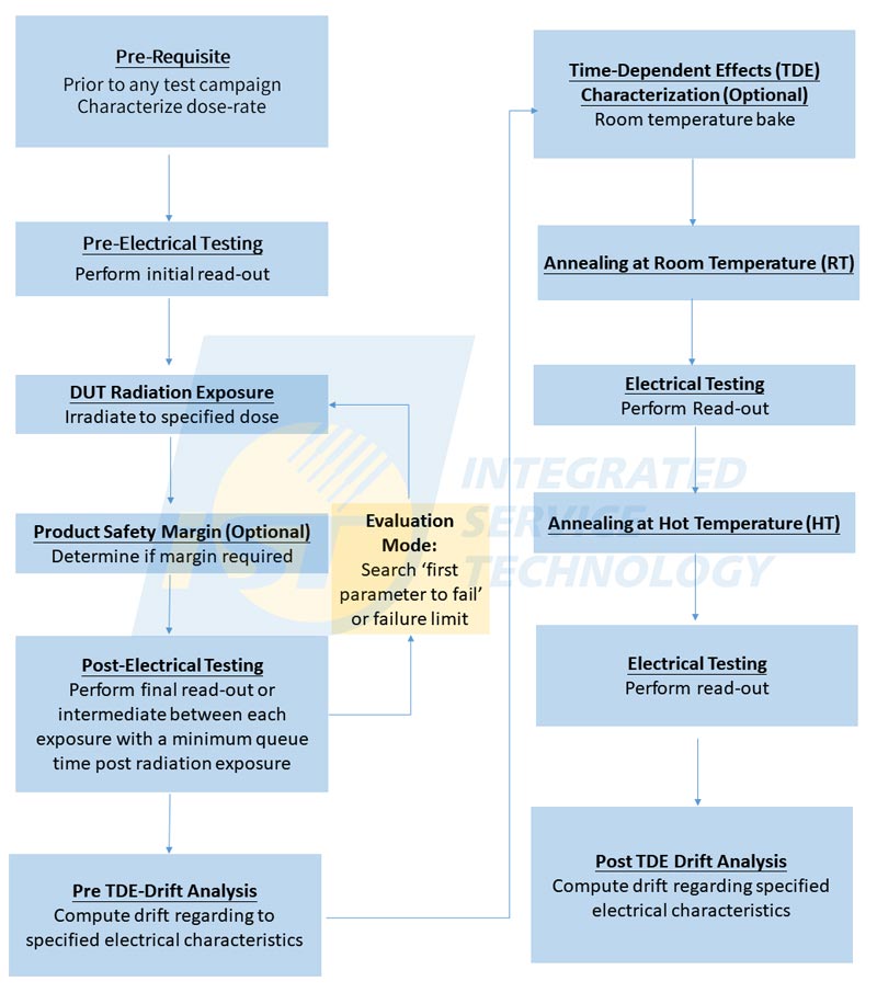
Figure 2: Flow-chart for TID characterization(Source:JESD22-B121)
- Supplier Limit Characterization
5. Final Report for X-ray Radiation TID Test
Samples have to be randomly selected from the parent population on a typical lot with a chosen quantity and additional unirradiated control samples.
The following items shall be contained in the final report for X-ray radiation TID test:
- Description of X-ray system, including:
a. Facility, vendor, model type, X-ray target type
b. X-ray setting and dose-rate
c. Filter thickness and material if filter is used
d. Distance between X-ray tube and test devices
e. Orientation in respect to the X-ray source - X-ray dosimeter description, including vendor, model type, dose-rate measurement range, and corresponding tolerance of accuracy range.
- Device description; including process node, product name, lot #, date code, etc.
- Package type and thermal-interface material type if any. In case of non-packaged unit (bare die or wafer level) or lidless/package decapsulated, this shall be noted.
- Total number of devices tested, including control (unirradiated) devices.
- Ambient temperature used for electrical testing.
- Time interval between exposure and read-out and annealing conditions in case of TDE characterization.
- The total amount of X-ray dose irradiated on each DUT:
a. Dose in air
b. Dose in material, if applicable
c. Dose conversion factor from air to material, if applicable
d. Characterization mode: failure limit or supplier limit - Electrical testing results.
- Description of X-ray system, including:
For devices such as metal-oxide-semiconductor (MOS) transistors, bipolar junction devices, non-volatile memories (NVM), flash memory/EEPROM, and dynamic random-access memory (DRAM), early failure due to parasitic radiation during 2D or 3D X-ray inspection is a growing concern—particularly in high-reliability applications.
To address this, iST offers a Parasitic Radiation Dose Deposition Validation Platform, enabling proactive evaluation of TID susceptibility prior to inspection. As a contributing member of the JEDEC JC-14.1 task group for the JESD22-B121 standard, iST utilizes high-sensitivity dose measurement systems and follows standardized test methodologies to accurately quantify radiation effects under specific X-ray conditions.
This process helps engineers determine whether the accumulated dose exceeds the design margin of the device, serving as a key reference for deciding whether further failure analysis or product screening is required. If you need additional information regarding parasitic radiation dose deposited verification platform, please kindly feel free to contact with Vick Chang, at +886-3-579-9909 #6566 │ Email: WEB_NDE@istgroup.com; marketing_tw@istgroup.com。