Issued Date: 2017/9/28
Issued By: iST
An IC on PCB failed yet it is back to normal after pressing it, what is up? Flawed IC Substrate? Cracked IC solder? Poor bonded wire?
Some, or all, of these may have baffled you as they share one common point:
It is either the IC chip or junction of IC packing or mounting that is flawed, and detection and testing can only be conducted without damaging the product (jeopardizing the crime scene).
iST Tech Classroom this month is going to present you a hot defect detection device in non-destructive way: the ZEISS Xradia 520 Versa high resolution 3D X-ray machine. Since its launch by iST last year, this hot hardware of zero-dead angle shooting and image surrounding has solved 1023 customer cases.
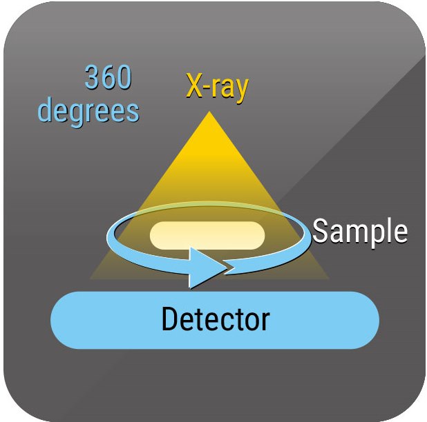
High Resolution 3D X-Ray Microscope is a non-destructive method employed with an optical microscope to enhance the magnification, which uses 2D X-ray tomography to take sample images at all angles while turning the fixed sample 360 degrees. Physical images of the tested object are then constructed by computer operation.
In the classroom this month, we are presenting you some of the key lessons we have learned from these 1023 3D X-ray cases.
Q1. Which products are suitable for 3D X-ray testing?
More important than easily identifying defects, the upgraded machine can now test more diversified samples in size and type. Scores of samples, including normal IC and 3D IC, MEMS, as well as PCBs, PCBAs, and finished products can be non-invasively tested at iST as long as they feature a footprint up to 30cm and weight up to 15 kilograms.
Q2. And which are not?
Limited by its physical characteristics, the X-Ray detection is not good for DUT containing high and low density materials at the same time.
That is, low atomic number, e.g. silicon die or AL wire in packed IC are hard to image since there are lots of high density substance, including substrate, lead frame (copper alloy), and cooling fin, in existence.
Q3. When and to what conditions should 3D X-ray be employed?
When and to what conditions should 3D X-ray be employed?
- Defect inspection during IC packaging such as inspections of wire bonding, plastic cracks, bubbles in epoxy or plastic, etc.
- Potential process defects in PCBs and carrier boards, such as circuit miss-align or bridge and open circuit, quality inspection of plated via process, multi-layer PCB layout analysis.
- Potential process defects in PCBs and carrier boards, such as circuit miss-align or bridge and open circuit, quality inspection of plated via process, multi-layer PCB layout analysis.
- Solder ball integrity inspection of BGA and flip chip packages, including solder ball deformation, crack, cold soldering, short, and blow hole.
- Crack inspection of high-density plastics or cavity inspection of metals.
- Inspection and analysis of active and passive components.
- Structure inspection of various materials.
Let us review some typical application cases!
Case 1: An IC on PCB failed often yet it is back to normal after pressing it?
Addressing this, we apply the non-lead solder point verification of the Temperature Cycling Test (TCT) to this IC on board until high resistance was detected; the follow-up non-destructive 3D X-Ray failure analysis then informs that the solder ball cracked.
Solder Ball Crack
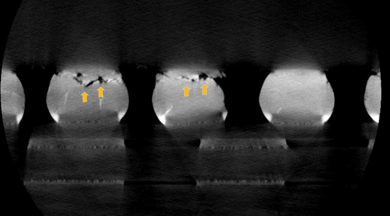
Case 2: Surface mounted large size IC failed to work as expected?
Large size ICs mounted to PCB tend to warp. The 3D X-ray informs that warpage results into a solder ball with open or head-in-pillow (HIP) symptom.
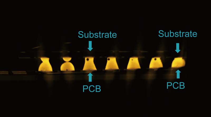
PCB Warpage & HIP
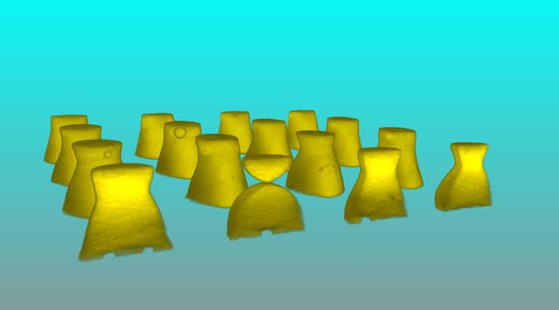
Head-In-Pillow, HIP
Case 3: Defects in IC substrate, crack or open?
Defects found in the PCB or via in inner circuit of IC substrate, with the help of 3D X-Ray it is clear that the via cracked.
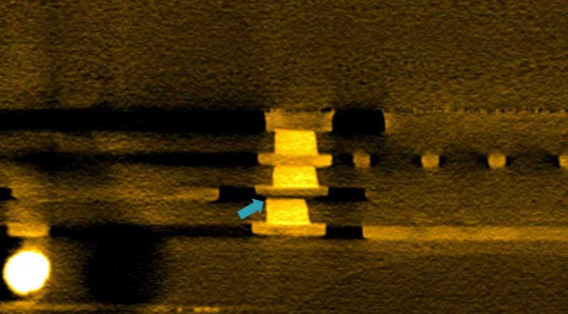
Via Crack
We are more than glad to share our inspection and test experiences with you. In case of any needs for abnormality inspection or determination suffered by your products or further information on 3D X-Ray, please call Miss Chen(Rita) at 03-579-9909 Ext. 6571 or Mr. Chang (Vick)at Ext. 6566 or send email to Email: web_nde@istgroup.com。