Issued Date:2022/11/22Nano-probing,
Issued By:iST
When a nanoscale chip fails, what type of electrical measurement should be applied to precisely locate a defect on such a tiny part?
Nano-probing
In recent years, most world-renowned companies are dedicated to the development of the 3nm/2nm process. Process technology is a never-ending competition. When encountering the bottleneck during the development, regardless of fields like IC design, wafer fabrication, test or assembly, defect analysis plays an essential role in clarifying the cause.
Failure analysis in advanced process is extremely critical to R&D as well as production stage. How to perform precise electrical characteristics measurement and defect localization on those interested transistors, which are only a few nanometers in size, poses a great challenge in recent semiconductor development..
Nano-Probing, consisting of nanoprobe and scanning electron microscope (SEM), is the answer to the aforementioned tasks. The integration of SEM at nm scale resolution and extremely small nanoprobe makes it possible to perform electrical characteristics measurement and fault isolation of nm scale transistor with precisely transistor positioning. Now, in this iST Classroom, we would like to share “How to apply nano-probing to defect localization.”
Nano-probing
Nano-probing
Connect the internal circuit or Via/Contact layer of an IC by extremely sharp and tiny probes (small radius of curvature) in SEM inspection system to enable the electrical characteristics measurement with applying input signals by external electrical characteristics measurement equipment. On the other hand, it is also possible to utilize the conductive property of metal layers to sense the absorbed electrons from emitted e-beam by SEM to perform the relevant application analysis, including EBIC (Electron Beam Induced Current), EBAC (Electron Beam Absorbed Current) and EBIRCH (Electron Beam Induced Resistance Change) analysis.
1. EBAC (Electron beam absorption current)
Figure 1 shows how EBAC works. When SEM’s e-beam scans the sample, the emitted electrons of scanning e-beam are absorbed by conductive metal routing on the analyzed sample. With applying the probe on the exposed area of the interested metal path, the absorbed electrons therefore are sensed by the amplifier (Amp) equipment to acquire the absorbed current. The absorbed current is hence constructed into a current image, which we call the EBAC image.
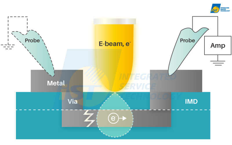
Figure 1: EBAC scheme
The bright zone on an EBAC image indicates the path of e-beam induced current. Once a dark area of current path on an EBAC image is observed, compared with reference or layout tracing, it indicates the probe cannot detect the current because it is “not a conductive path” or “open failure”. Generally, the boundary between the bright and dark zones of current path is the site where an open fault is isolated.
Secondary electron (SE) image in SEM reflects the topography of a device under test (DUT). By overlaying the EBAC image on the corresponded SE image, it is possible to trace current path on the DUT surface. This method of measurement enables to check the path integrity of the interested electrical path. If the interested electrical path is open, we can precisely isolate the fault with comparing good and bad parts or layout tracing.
Figure 2 is a fault isolation example by EBAC analysis: the left image shows the circuit layout and the right one is the corresponded EBAC image with overlaid on the SEM secondary electron image. The bright zone represents the current path when the e-beam is absorbed by conductive path and the parameter analyzer of nanoprober measures the absorbed current. Compared to Figure 2 (left), we can clearly see the bright current path of probed path. The nanoprober in iST failure analysis lab is now available for you to implement such analyzing method to determine if there is any open or short issue on interested electrical paths.
In this case, we can observe the in-completed current path, boundary between bright and dark area of current path, is located on the left-bottom portion, which is open fault location of the analyzed path. Besides of the measurement on BEOL metal paths, EBAC can also be applied to isolate abnormal leakage current fault isolation on gate oxide breakdown issues.
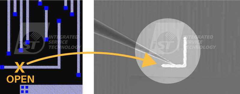
Figure 2: Example for EBAC analysis
(left): Circuit layout of nano-probing analyzed area;
(right): Corresponded EBAC image overlaid on SEM secondary electron image2. EBIC (Electron beam induced current)
EBIC is the analysis to measure the induced current by emitted e-beam from SEM systems, especially in P-N junction (illustrated in Figure 3). A “depletion region” forms in the P-N junction and a “build-in electric field” is then created in this region.
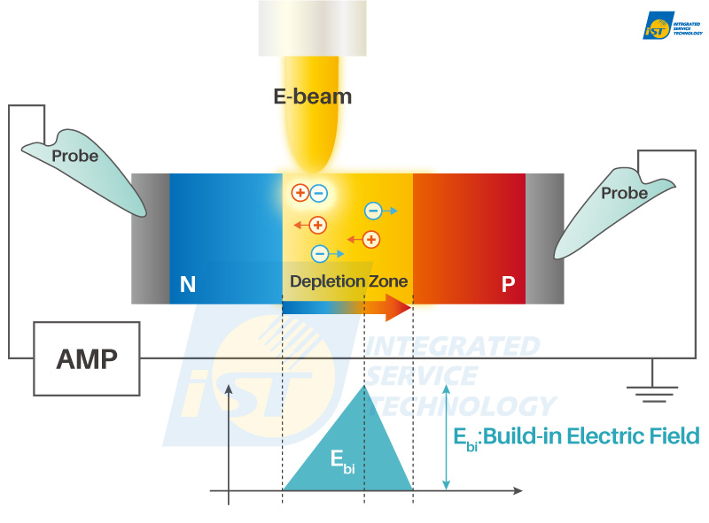
Figure 3: EBIC scheme
While scanning the P-N junction on sample surface, the e-beam is induced to generate electron-hole pairs in depletion zone. Taking Silicon for example, most common material in semiconductor field, the required energy to generate electron-hole pairs is 3.6eV. The electron-hole pairs are then separated by the built-in electric field of the depletion region and sensed by the amplifier through nanoprobes, and eventually forms a current image.
EBIC can be employed to analyze characteristics in P-N junction, such as the information of built-in electric field intensity, or the diffusion length calculation of carriers by the measured current intensity. Such information is very helpful for material characteristic analysis.
3. EBIRCH (Electronic beam induced resistance change)
The principle of EBIRCH is quite similar to OBIRCH (optical beam induced resistance change); the only difference between these 2 techniques is the scanning source difference. The scanning source of OBIRCH is “optical laser beam” with a µm-level spatial resolution with laser wavelength. While scanning source of EBIRCH is “electron beam” that enhances spatial resolution to nm-level with a wavelength much shorter than laser and thus can precisely locate the defect as well as significantly improve the success rate of the following physical failure analysis, including TEM (transmission electron microscopy) analysis to reveal the fault of analyzed sample.
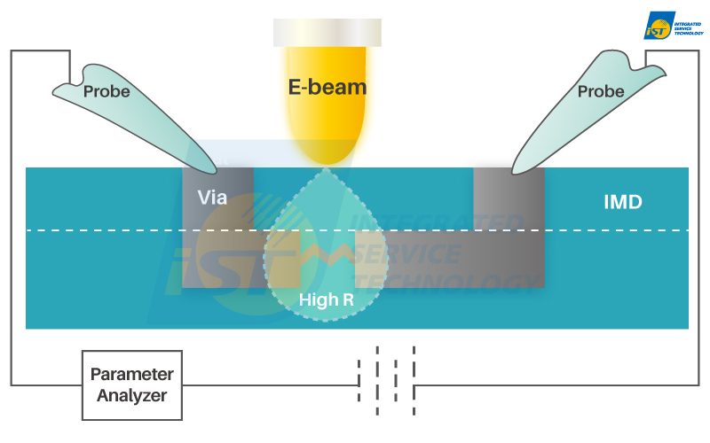
Figure 4: EBIRCH scheme
With the combination effect of temperature properties of different material and Seebeck effect, resistance difference caused by faults can be detected by the scanning e-beam on the analyzed sample. We can hence locate the defect position by comparing the good/bad samples.
When implementing EBIRCH analysis, we can apply different bias conditions to achieve an optimized condition for precise fault localization. EBIRCH is a powerful analysis, which is suitable for short circuit, leakage and high-resistance failure analysis.
In Figure 5, it is a case that leakage failure is measured by nanoprober IV analysis. With implementing EBIRCH analysis (Left of Figure 5) and overlaying EBIRCH on the secondary electron image, the fault is precisely isolated on the defective contact (Right of Figure 5) . The EBIRCH finding facilitates precise positioning in PFA or TEM analysis thereafter.
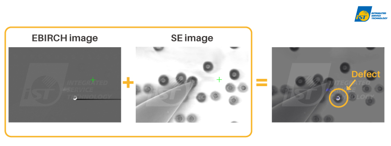
Figure 5: Precisely locate the defective contact by overlaying EBIRCH on secondary electron image.
With the continuous development and evolution of nm-scale process in the semiconductor industry, iST also keep proactive pace to agilely integrate the nano-prober system and develop corresponded FA solutions to achieve accurate fault isolation and electrical characterization for the analyzed samples in order to solve customers’ product issues.
In case you have any needs or want to learn more about what it is all about, please contact us at +886-3-579-9909 Ext. 6780 or 6788 Shaun Chiu│ Email: web_EFA@istgroup.com;marketing_tw@istgroup.com
Other services you may be interested in
Nano-probing