Issued Date:2024/3/19 Flying Probe
Issued By:iST
When issues arise with a product, is it due to component aging or defects occurring during the assembly process onto the PCB? How can we clarify this distinction and effectively troubleshoot the defects?
Flying Probe

With the flourishing development of applications such as AI and HPC (High-Performance Computing), IC manufacturers are continuously striving to develop powerful and compact 3D stacked heterogeneous integration chips. The PCBs (Printed Circuit Boards) carrying these chips often exhibit characteristics of high density and multiple layers, resulting in significantly high hardware costs and placing extremely high demands on the quality of electrical properties.
In light of this trend, the semiconductor industry has embraced a key technology: Flying Probe Testing. This technology not only assists IC development engineers in conducting initial quality checks during the PCB and PCBA (Printed Circuit Board Assembly) stages but also enables monitoring of component-on-board quality after reliability stress testing. In case of defects detected during reliability testing, it can swiftly pinpoint the root cause of anomalies occurring after component mounting on the PCB (PCBA), whether it’s due to components or hardware issues, thereby saving time and costs in time-to-market.
Flying Probe Testing is equally applicable in the automotive market, particularly in situations where ensuring product quality and personal safety is paramount. Automotive electronics manufacturers are more willing to invest in costs to ensure products pass qualification the first time, thereby avoiding unexpected defects that could result in customer returns or recalls. Furthermore, when facing various tests involving high temperatures, humidity, and vibrations, Flying Probe Testing can provide numerical comparisons of PCBs before and after the tests, reducing the possibility of human measurement errors and enhancing the quality of qualifications.
In this edition of iST Classroom, we will share with you the optimal timing for using Flying Probe Testing through practical case studies, as well as how it can assist engineers in the rapidly changing semiconductor market. With its characteristics of high efficiency, accuracy, and wide test coverage, combined with data analysis, Flying Probe Testing not only enhances the quality of Burn-In Boards (BIBs) but also further improves the pass rate of subsequent reliability tests.
Flying Probe
Flying Probe
1. The Principles and Types of Flying Probe Testing
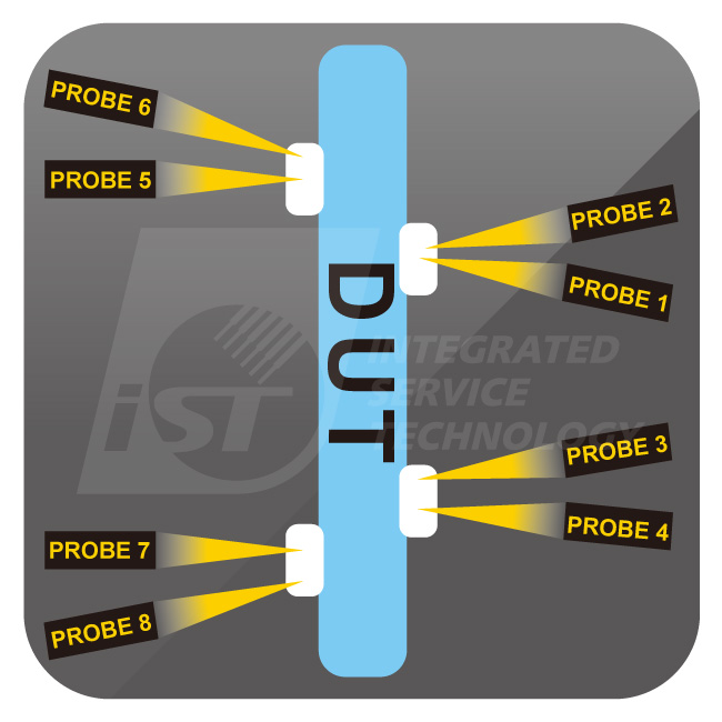
Flying probe testing can be divided into two main types:
(1) BBT Flying Probe Testing
Flying probe testing for bare PCBs, referred to as BBT (Bare Boards Test), involves conducting continuity measurements using flying probes on PCBs that have not yet had components mounted. This process aims to identify defects such as opens and shorts between each circuit, thereby enhancing product reliability inspection.
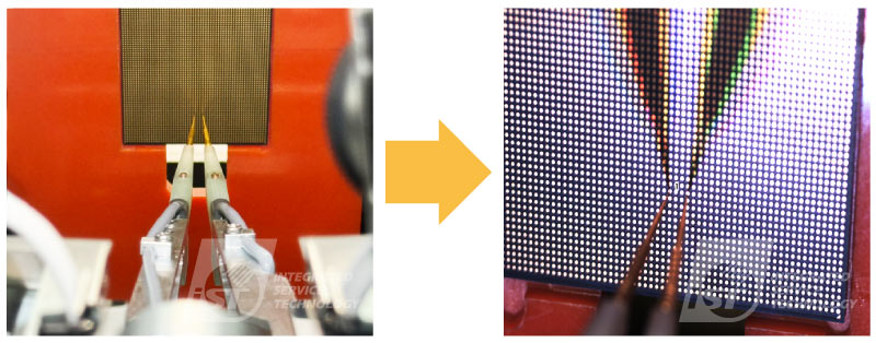
Figure 1: BBT Flying Probe Testing. (Source: iST)
(2) ICT Flying Probe Testing
ICT Flying Probe Testing, abbreviated as ICT (In Circuit Test: PCB with components), refers to test PCBs with components already mounted, which is a key application of flying probe testing. It enables precise measurement of various electrical values between component pins and solder joints, accurately distinguishing between good products, open or cold solder joints, and component abnormalities. The scope of ICT testing includes various components, primarily including resistors, capacitors, diodes, MOSFETs (Metal-Oxide-Semiconductor Field-Effect Transistors), jumpers, relays, and voltage regulators. This testing method allows for determining whether individual components on the PCB have failure occurring during the assembly process, providing important test data to ensure manufacturing quality and proper functioning of components.
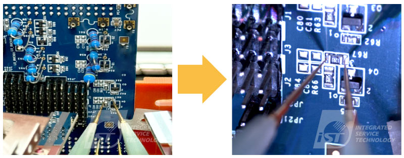
Figure 2: ICT Flying Probe Testing. (Source: iST)
2. Advantages and Applications of iST’s Flying Probe Testing
Below, we will outline how iST ICT flying probe testing service provides engineers with fast testing and feedback during the reliability testing phase, thereby shortening product time-to-market and enhancing competitiveness.
(1) The Three Key Advantages of iST’s ICT Flying Probe Testing
- No Need for Custom ICT Fixtures:
iST’s ICT flying probe testing program software is highly flexible and can quickly adapt to various requirements. There is no need to develop custom ICT fixtures to complete PCBA testing. Even when the PCBA needs to be modified or when certain passive components need to be added or removed, there is no need to modify the fixtures, thus saving a lot of time and reducing additional cost expenses. - High Test Coverage:
iST’s reliability laboratory achieves relatively high ICT flying probe test coverage through appropriate test program and fixture designs, ensuring comprehensive testing. Particularly in the face of challenges posed by hardware interference during PCBA functional testing and connectivity testing, well-designed test programs and fixtures are key to increasing coverage. - PCB Deformation Compensation Mechanism:
Considering the possibility of minor deformation (warpage) during PCB manufacturing that may affect flying probe testing, iST’s ICT flying probe testing utilizes laser scanning technology. This technology compensates for probe penetration depth by scanning PCBs in sections when there is bending, ensuring the accuracy and reliability of flying probe testing.
(2) Four Key Timing for Using Flying Probe Testing
- Verification of Component Functionality in the Manufacturing Process:
Flying probe testing can be utilized after surface-mount technology (SMT) assembly of passive and active components. Through tests such as power-on testing, connectivity testing, and component testing, it ensures whether the components are functioning properly, thereby avoiding the use of damaged or faulty components in tests. It also helps identify and filter out problems with components on the assembled PCB (PCBA), increasing manufacturing yield and further ensuring overall quality in the reliability testing. - Troubleshooting:
In case of defects during test, flying probe testing can assist in troubleshooting the assembled boards. When component quality concerns arise, or when running different batches of test units with the same boards. The flying probe test record before the tests (T0) can be used to compare and analyze any data discrepancies. Additionally, ICT flying probe testing is also applicable for inspecting and repairing faulty boards during rework processes. - Aging Status Check of Burn-In Boards (BIB):
After undergoing high-temperature test for a period of time, both the boards and components may inevitably experience aging issues. Flying probe testing can be used to compare the test data before the tests to identify aging components. - Test Phase:
In the qualification of automotive electronic products. The Board Level Reliability (BLR) tests aim to evaluate the reliability and durability of semiconductor components after surface-mount technology (SMT) assembly. During this phase, ICT flying probe testing can also be utilized to compare measurement values before and after tests. For tests involving high repeatability such as high temperature, high humidity, and high vibration tests, ICT flying probe testing can quickly conduct measurements. Consequently, it is less affected by external environmental factors and changes, optimizing the reliability and quality of the manufacturing process.
- No Need for Custom ICT Fixtures:
3. Cases Sharing
Next, we will share how iST’s reliability laboratory utilizes ICT flying probe testing to identify defects on components mounted on PCBs. Below, we will illustrate this through four major case studies.
(1) Pin-to-Pin Short Circuit Issue
When abnormalities such as circuit short are discovered in a product, it is necessary to confirm whether it is due to defects in the PCB itself or caused by components. In this case (Figure 3), it is a Pin-to-Pin short circuit issue, which is difficult to identify with the visual inspection. However, by using flying probe testing to test the circuits on the PCB, it is easy to pinpoint which circuit has a short circuit. In comparison, manual inspection would require a significant amount of time and cost. Utilizing a flying probe machine can quickly and accurately detect the problem.
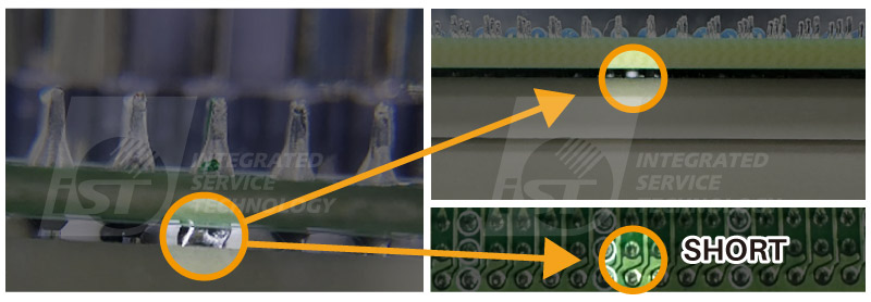
Figure 3: Pin-to-Pin solder overflow abnormality that is difficult to detect with the visual inspection, but can be quickly identified by flying probe testing. (Source: iST)
Another case (Figure 4) involves defects of short circuit found on the pins of a socket (chip test socket). After using flying probe testing to rule out the abnormalities on the PCBA, it was ultimately discovered that the issue lied with the socket.
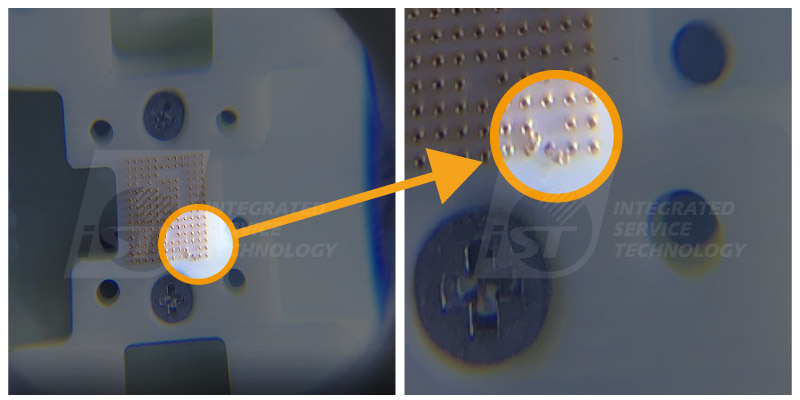
Figure 4: Flying probe testing can quickly rule out PCB issues and identify the root cause of the short circuit. (Source: iST)
(2) Passive Component Damage Results in Abnormal Resistance Values
Damage to passive components on the PCBA can result in abnormal resistance. Using conventional methods to customize ICT testing fixtures can take days to weeks. However, by employing ICT flying probe testing, probes can accurately contact with test points on the components under test, enabling rapid measurement of passive components (resistors, capacitors). This approach swiftly identifies whether component values are abnormal.
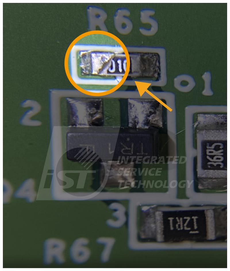
Figure 5: The component damage leads to abnormal resistance values. (Source: iST)
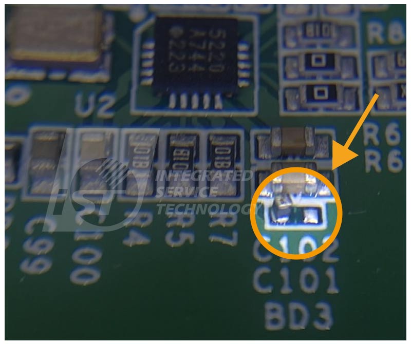
Figure 6: The capacitor tombstoning results in abnormal capacitance values (Source: iST)
(3) Mis-assembly of Jumpers Results in Abnormal Continuity
In advanced manufacturing processes, electronic components on PCBA are typically intricate and densely packed. Even the absence of just one jumper can result in defect. In such cases, using flying probe testing for open and short circuit tests provides a precise method to test the connectivity between various connection points, allowing for the rapid and effective identification of the issue. Once the problematic open or short circuit points are identified, resolving the problem merely requires replacing the jumper, eliminating the need for extensive inspection of the entire PCBA. This saves time and labor costs.
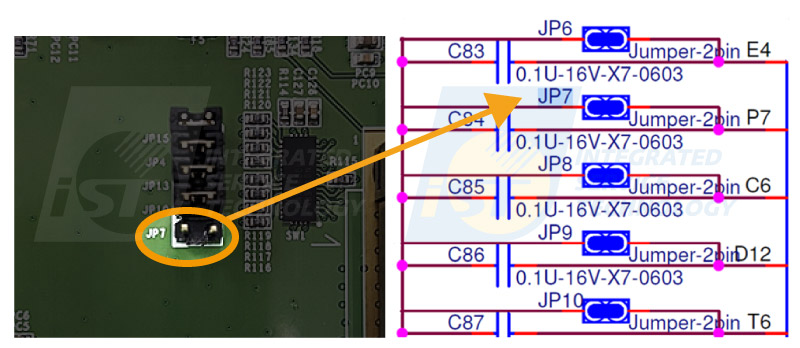
Figure 7: The absent jumper results in abnormal connectivity values. (Source: iST)
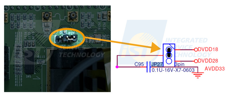
Figure 8: The mis-assembled jumper results in abnormal connectivity values. (Source: iST)
(4) Soldering Issue Results in Abnormal Voltage Values
During iST’s reliability laboratory’s ICT flying probe testing for voltage regulator measurements. The flying probe machine has the capability to detect abnormalities in conductivity. This allows for the precise identification of soldering issue on the IC pins.
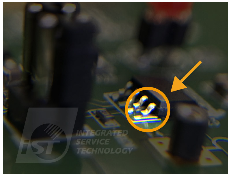
Figure 9: The soldering issue results in abnormal voltage values. (Source: iST)
iST’s reliability laboratory observes that with the continuous evolution of advanced manufacturing processes and new technologies, IC stacking technology is becoming increasingly mature. Against this backdrop, more and more consumer electronics or automotive electronic IC manufacturers have adopted ICT flying probe testing technology, leveraging its high efficiency, accuracy, and broad test coverage characteristics. Combined with data analysis, this has effectively increased the localization rate of failure components and the pass rate of subsequent reliability verifications.
We appreciate the ongoing support from you all. If you would like to further understand the details, please feel free to contact Mr. Yen at +886-3-579-9909 ext. 6461 or via email web_rce@istgroup.com;marketing_tw@istgroup.com