Issued Date:2024/6/18 AI chip RA challenges
Issued By:iST
Don’t want to be left behind in the AI era? Ensuring chip quality and reliability is crucial. AI chips face three major challenges: ultra-high-power consumption, ultra-low voltage, and heterogeneous integration. Do you know how to tackle them?
AI chip RA challenges
At a recent launch event, OpenAI and Google unveiled their flagship models, “GPT-4o” and “Project Astra.” These advanced models not only allow users to exchange text, images, and audio in conversations, but the robot at the other end can also describe the user’s surroundings through the phone screen and infer the user’s emotions from their tone. When the conversation gets joyful, it can even laugh and sing, making communication almost indistinguishable from interacting with a real person.
The AI technology is used to retrieve object characteristics parameters and make judgment based on human brain simulation by replicating neural network and deep learning. It may seem complex, but AI technology has already integrated into our daily lives, from generative content and autonomous driving to smart homes and healthcare. Its wide-ranging and promising applications span finance to manufacturing. AI is poised to continue leading innovation, becoming a key driver of industry development.
In addition to supporting algorithm and big data evolution, AI chips are moving in big and fast paces toward high performance, high bandwidth and low power consumption as required by different application domains (Table 1). However, these features not only impact the performance and lifespan of AI chips but also pose significant challenges to the design methods and equipment for AI chip reliability testing. iST’s Reliability Verification Laboratory has identified the three most common challenges for AI chips and their solutions. In this iST classroom, we will explain each of these challenges in detail.
AI chip RA challenges
AI chip RA challenges
1. The Three Most Common Challenges for AI Chips
(1) The Challenge of Super High-Power Consumption by Cloud AI Chip: Thermal Dissipation and Balance
The cloud AI chips deployed in data centers are set to deep learning so the computing performance must be raised. This results in huge power consumption (over 200W by single chip) which, in turn, it will generate substantial heat that accelerate the aging process of the chips.
Therefore, for cloud computing AI chips that must operate continuously 365 days a year, the reliability issues caused by aging need to be carefully evaluated. AI chip RA challenges
The principle of reliability testing involves sampling a certain number of IC to predict the lifespan and failure probability of the entire population. Typically, 77 chips are sampled. When these 77 high-power chips undergo a 1000-hour reliability test in a single system, the resulting tens of thousands of watts of power will severely test the system’s thermal dissipation and thermal balance capabilities.
Only with precise thermal dissipation and thermal balance can each chip maintain a stable junction temperature (Tj) while performing various computational modes. This stability is crucial for accurately predicting the IC’s lifespan. Therefore, managing and controlling the heat generated by high-performance cloud AI chips is a significant challenge in the design of IC reliability experiments.
(2) The Challenge of Super Low Voltage by Edge AI Chip: Limit of Reliability Verification and Hardware Solutions Imposed by Multi-System Power Requirements
In addition to requiring high computational performance, edge AI chips must also feature low power consumption to meet the demands of their application environments. For instance, mobile devices, Internet of Things (IoT) devices, drones, and electric vehicle autonomous driving assistance systems all rely on battery power, making low power consumption design crucial.
As semiconductor processes continue to advance, the dynamic current consumption for the same number of logic gates has become increasingly efficient. However, the physical effects of miniaturization have led to an increase of the static leakage current of transistors. According to Moore’s Law, the area of transistors can be reduced by half every two years, but this does not correspondingly reduce the power density of chips. As a result, chips of the same area will consume more electrical current than before.
To reduce power consumption, in addition to adopting low operating voltage designs, multi-operating voltage and multi-gate voltage designs are also very common. However, for reliability testing systems, the demand for more than 10 power supplies at a time challenges the limits of the power supply capacity of reliability testing equipment.
Simultaneously, with core power operating at 1V or even lower, the power margin for ICs becomes smaller. This makes voltage drops (power IR drops) and power ripple on the circuit board more likely to cause errors in IC reliability testing. Voltage drops occur not only in the main power supply but also require the voltage levels of some logic gate signal sources (patterns) to be reduced in tandem with the main power supply. This further complicates hardware design and testing, posing significant challenges to the reliability testing system’s capabilities and hardware design.
Thus, planning a High Temperature Operating Life (HTOL) reliability testing environment that meets the needs of edge AI chips requires meticulous attention to every detail and design consideration, from equipment selection to PCB circuit board simulation and production. This process is inherently more rigorous compared to standard logic ICs.
(3) The Challenge of Heterogeneous Integration: Complex Heat Dissipation Path
AI chips are trending toward heterogeneous integration. This integrates heterogeneous chips of different processes into one package to speed up transmission bandwidth among them as found in components of HBM, sensor, MEMS and antenna. Chips are aligned or stacked (Figure 1) by processes including TSV, RDL, bump and interposer for better data transmission efficiency and lower power consumption among heterogeneous chips.
This comes at a price. That is, a complex heterogeneous packaging stacking structure would complicate the ways that heat gets generated and dissipated. Take as an example: Chips of greater power consumption may go off the center of the packaging and the chips may come with different thicknesses. All these would make the heat dissipation and thermal sensing of the chip different from the traditional packaging and complicating the measurement and temperature monitoring operations throughout the reliability verification period.
Based on the above, addressing the challenges of heat dissipation and thermal balance, the voltage limits of the testing system, and the complexities of thermal dissipation paths in heterogeneous integration are critical when performing reliability design verification. In response, iST Reliability Verification Laboratory offers the following recommendations.
2. How to Overcome the Reliability Challenges of AI Chips
(1) Steadily Control Heat Generated by AI Chip of High-Power Consumption with a Liquid Cooling System
Thermal Design Power (TDP) is a specification that outlines the cooling capacity requirements for a CPU on a motherboard. Currently, the TDP specification for desktop CPUs is around 150 watts (W) at its highest. Gaming enthusiasts tend to upgrade mother board, heat sinks, fans and other accessories to keep the CPU running at high efficiency and frequency over extended periods. These upgrades enhance the system’s cooling capacity beyond the TDP requirements, allowing the CPU to operate at high frequencies for extended periods without encountering issues such as overheating, throttling, or entering sleep mode. AI chip RA challenges
However, for server and HPC (High-Performance Computing) cloud AI chips, the current TDP specification has exceeded 200W, resulting in extremely high heat dissipation requirements. Due to the packaging structure and material factors, it has become increasingly difficult to use air convection as a cooling medium to maintain the chip junction temperature within the target range.
Especially in reliability testing, the target temperature is set at 125°C, way above the 70°C required by desktop computers. In most cases, at 125°C, the chip’s power wall is unlocked, making the chip highly susceptible to thermal runaway due to high temperatures. Therefore, when conducting high-temperature reliability testing on ICs with such high-power consumption, the testing system must provide faster heat dissipation capability.
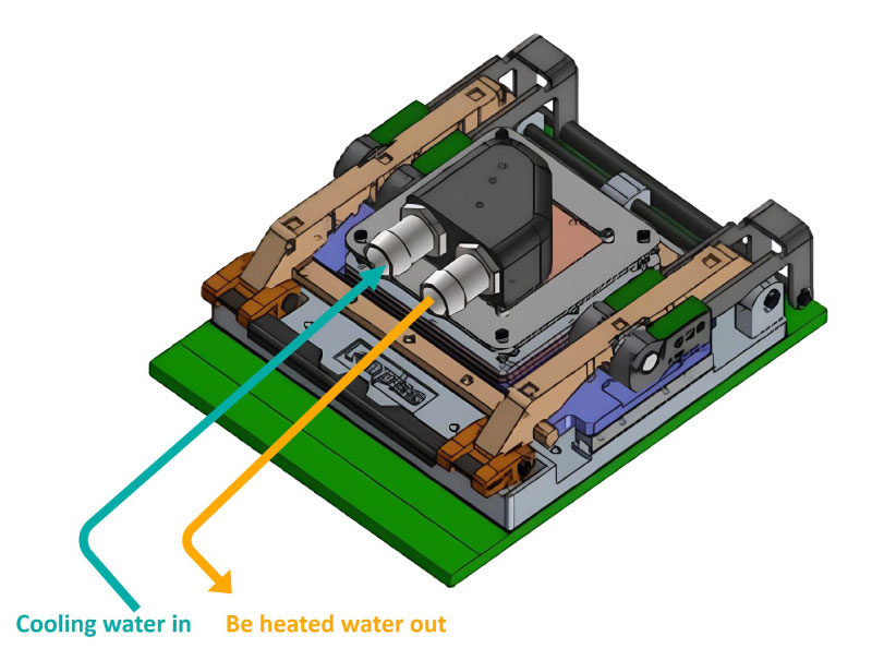
The solution proposed by the iST’s Reliability Verification Laboratory is to utilize a more efficient liquid cooling system, paired with custom liquid circulation sockets (Figure 2). This system takes advantage of the superior heat exchange rate of liquid compared to gas, as well as methods such as real-time monitoring of chip’s temperature and adjusting liquid flow rate to stably control the heat generated by ultra-high-power AI chips, successfully collecting reliability test data.
(2) Pre-simulation on Burn-in Boards in Advance to Prevent Poor Performance after Assembly
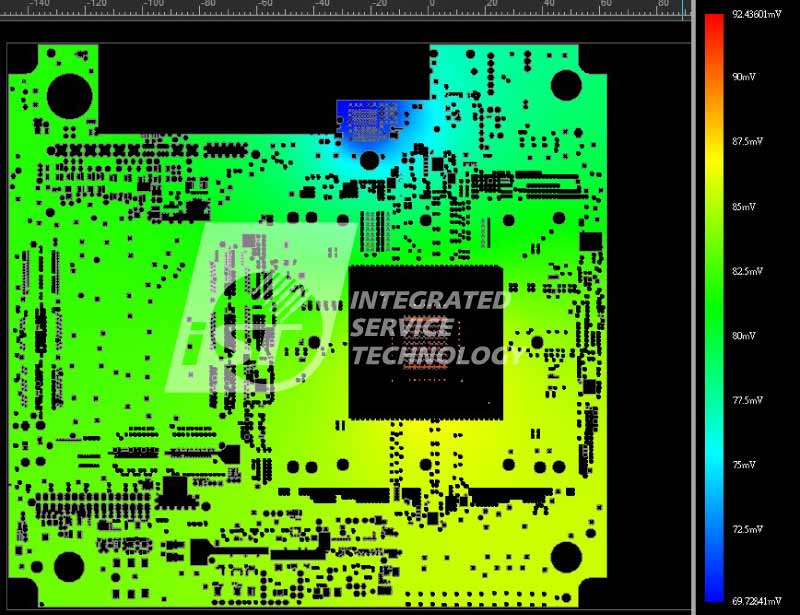
AI chips are now utilizing advanced processes, with operating voltages dropping to below 1V. However, when high currents flow through the PCB traces, it can easily generate voltage drops (DC IR drop) across the board, as shown in Figure 3. This IR drop can decrease the already low operating voltage, potentially causing AI chips to fail due to insufficient power voltage margin.
Moreover, when IC power draws large currents, it can also produce various frequencies of simultaneous switching noise (SSN).
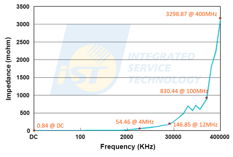
Different PCB layout may result in various power plane impedance value (Figure 4) by different load frequencies. When the impedance exceeds the target value at a certain frequency, it can result in severe power AC noise and power ripple, leading to AI chip failure due to inadequate power noise margin.
Furthermore, in traditional circuit board design, placing multiple chips on the same board makes it difficult to achieve consistent wiring layout for each chip. This leads to differences in electrical testing between chips and increases the complexity of design and testing.
To address this issue, iST’s Reliability Lab adopts a new design concept for Burn-in Module (BI module), breaking away from traditional circuit board design thinking. Instead of testing multiple chips on a single board, the circuit board is downsized to test only one chip. Coupled with various wiring layout tools available, adjustments can be made during the early stages of reliability circuit board design through software analysis and simulation. This includes optimizing factors such as the length and width of power lines, the size and number of plated-thru holes, decoupling capacitor values, and their placement to address issues like IR drop and power layer impedance. By doing so, it prevents the occurrence of performance issues encountered only after the completion of production assembly. Moreover, downsizing the circuit board to a single chip allows for more experimental parameters to be obtained for each Device Under Test (DUT) during aging tests. It also enables individualized test parameter settings based on the different static leakage currents of each chip’s transistors, further enhancing the testing quality of AI chips.
(3) Tailor-Made Jigs to Fit Dies of Different Thickness
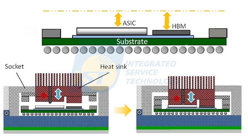
Heterogeneous integrated AI chips may come with dies at different thicknesses. This mandates jigs for the reliability verification featuring chip-specific IC socket, heat sink and sensor to fit dies at different heights for better heat dissipation and more accurate temperature measurement and monitoring (Figure 5).
(4) Using Thermal Diode Circuit to Monitor the Internal Temperature of ICs
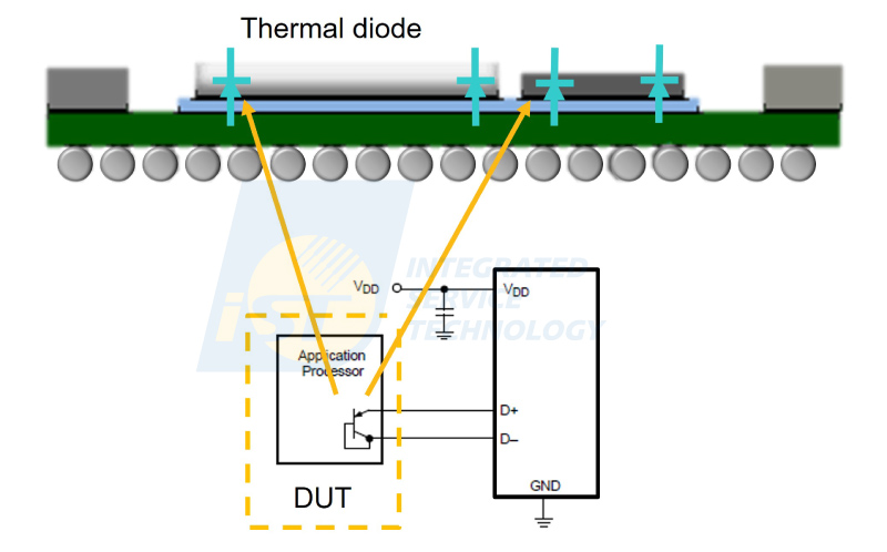
The high-power consumption of cloud-based AI chips can lead to unexpected failures during reliability testing, such as thermal runaway, due to rapid temperature fluctuations within the chip itself. Therefore, when the IC incorporates a thermal diode component, iST’s reliability verification laboratory can customize the thermal diode monitoring circuit to monitor the internal temperature of the IC, allowing for real-time and accurate measurement of the junction temperature (Figure 6).
This approach offers fast response times and, when combined with the highly efficient liquid cooling control adjustment system mentioned earlier, is more suitable for rapidly changing temperatures in ultra-high-power AI chips, thereby providing real-time heat dissipation. In addition, the thermal diode monitoring circuit can independently measure the temperature of each chip in multi-chip structures, such as 3D packaging, to achieve more accurate reliability data collection.
3. Quick Reference Guide for AI Chip Reliability Solutions
To summarize the issues and solutions discussed above, iST’s Reliability Verification Lab has created a comprehensive table (Table 2) based on years of experience. This table provides a quick overview of the solutions for different reliability challenges faced by AI chips.
Based on its hands-on experiences from consumer chips, automotive chip, 5G chips and the AI chips now, the iST’s Reliability Verification Lab is confident to tackle the issues of super high power, super low voltage and heterogeneous integration faced by AI chip when designing a reliability verification. The lab is committed to providing you with reliability verification data (e.g., accurate temperature and voltage value) to improve the reliability of AI chips.
Thank you for your continued support of iST. If you have further questions or need assistance, please feel free to contact Mr. Bear Hsu at +886-3-579-9909 ext. 6428 or via email at web_cre@istgroup.com ; marketing_tw@istgroup.com


