Issued Date:2020/6/5III-V Materials
Issued By:iST
The application of techniques utilizing transmission electron microscopy (TEM), scanning transmission electron microscopy (STEM) and energy dispersive spectroscopy (EDS) to identify the interface and defect property in GaN based materials is presented. Several parameters including STEM camera length and probe size were demonstrated to have significantly influence on image contrast and layer thickness, respectively. The dislocation, localized strain and polarity of GaN were also reviewed in this work. By choosing the optimized parameters, rapid and accurate analysis of detail structural and electronic information could be obtained.
III-V Materials
I. INTRODUCTION
With increasing demand in the market, GaN based III-V materials are fabricated into high brightness light emitting diode (LED) and laser diodes (LDs) [1]. The optoelectronic properties of both devices are susceptible to the morphological and composition fluctuation of the epitaxial area, including p and n type doping GaN, and multi quantum well (MQW) structure. The layer thickness and defect property such as strain field will dominate the internal quantum efficiency (IQE), which for example will be reduced by the indium segregation [2]. Therefore, effective methodology to characterize the detail structural information attracts great interest in the material analysis community [2-3].
Among those common techniques applied to analyze III-V materials, including scanning electron microscope (SEM), secondary ion mass spectrometry (SIMS) [4] and photoluminescence (PL), TEM can be used to obtain both the detail structure and composition information at the same time, which make it necessary to gain the full understanding of the III-V materials. Besides the regular morphological observation, other novel techniques could also be equipped on TEM as well, such as nanocathodoluminescence (nanoCL) for doping condition investigation [5], and in-situ TEM for atomic scale characterization of III-V semiconductor growth [6].
In this study, we demonstrate some TEM/STEM techniques toward the III-V materials analysis, except the common TEM/STEM images, advanced techniques such as nano beam diffraction (NBD), convergent beam electron diffraction (CBED) and two-beam condition were applied to determine the local strain and polarity.
II. EXPERIMENTS
The STEM NBD and EDS data was collected in JEOL JEM-2800F TEM (200kV) equipped with dual silicon drift detectors (SDDs) [7]. The center dark field (CDF) TEM image and and CBED pattern were conducted using JEOL JEM-2100F TEM (200kV). The focus ion beam (FIB, FEI Helios 660) was used to prepare all the TEM samples at 30kV and lower kV for U cut and final clean, respectively.
III. RESULTS AND DISCUSSION
A. High angle annular dark field (HAADF) image contrast
With the annular dark field detector, HAADF obtains inelastic scattering electrons at high collection angle, which also implies that the image intensity of HAADF will be dominated by atomic number (Z), so that it can produce better elemental contrast than bright field (BF) and conventional TEM modes [8].
In the present study, HAADF was conducted to characterize the layer thickness of AlGaN. Figure 1 shows comparison between the HAADF image, STEM BF image and TEM BF image. The contrast of AlGaN in p-GaN and interlayer are significantly enhanced in HAADF mode, which makes it a powerful tool for the composition related analysis.
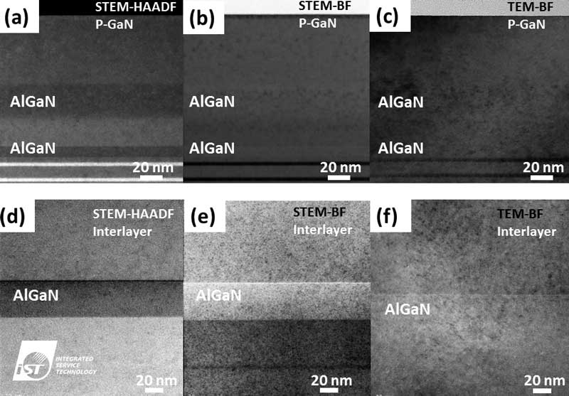
Fig. 1 The comparison of the image contrast between HAADF mode (Fig. 1a and 1d), STEM BF (Fig. 1b and 1e), and TEM BF (Fig. 1c and 1f).
B. STEM/EDS analysis
The JEM-2800F TEM with dual SDD system was applied in the present work to demonstrate the possible artifact during the STEM/EDS analysis of InGaN/GaN multi quantum well (MQW) structure. The uniformity and distribution of the indium atoms were characterized utilizing EDS line scan with three different STEM probe sizes to verify the corresponding spatial resolution.
Figure 2 shows that the EDS line scanning profile using 0.2 nanometer probe can resolve the InGaN layers with full width at half maximum (FWHM) of 3.3nm, which is almost the same result as the STEM BF image. In contrast, the condition of one nanometer probe obtained over ten times counts higher than the 0.2 nanometer one but with the loss of resolution. However, with a well design, high efficient EDS system, the resolution can be maintained by using the fine probe while the sufficient counts for data interpretation can be collected and keep sample from electron beam damage at the same time, especially for the beam sensitive material, such as indium [2].
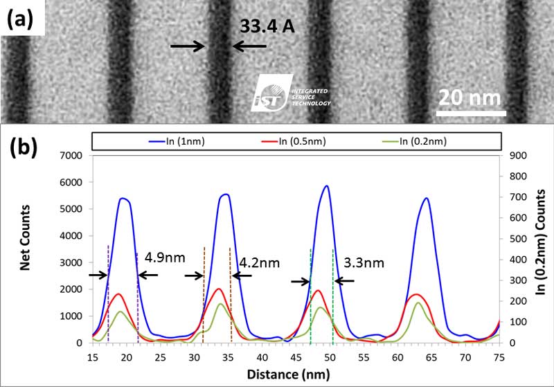
Fig. 2 (a) The STEM BF image of the InGaN MQW structure, and (b) the corresponding EDS line scan profile of In distribution.
C. Strain field analysis by nano beam diffraction
The nano-beam diffraction (NBD) technique operated at STEM mode was utilized for the strain analysis of MQW structure. The detail function and working principle can be found in our previous work [9]. Figure 3 shows the strain mapping result of the MQW, which indicates that certain amount of the compressive strain was found in the GaN barrier, while small strain field was built up in the InGaN well.
In comparison, TEM center dark field in two beam condition was applied to verify the result of strain map in fig. 3a. From fig. 3b, the diffraction contrast of strain field was found both in the well and barrier layers, which confirms the result of NBD technique.
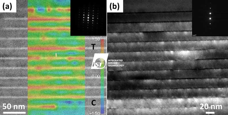
Fig. 3 (a)The strain map of the InGaN/GaN MQW structure, and (b) the corresponding TEM center dark field image.
D. Convergent beam electron diffraction
The local crystal structure can be examined by CBED technique from the variation of regional diffraction condition, which can be used to determine the local strain [10]. The strain can, on the other hand influence the device efficiency and reliability severely. Therefore, it is required to have a close study regarding the strain field in each layer of III-V material, especially the quantum well structure.
We demonstrate here the CBED pattern obtained on the (10-10) zone axis in TEM mode, which allows us to determine the polarity along [0002] direction by comparing the high order Laue zone (HOLZ) line patterns.
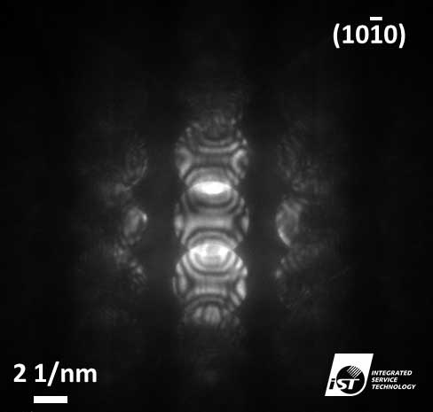
Fig. 3 (a)The strain map of the InGaN/GaN MQW structure, and (b) the corresponding TEM center dark field image.
IV. CONCLUSION
TEM/STEM applications are present here to demonstrate the efficient and accurate methodologies to fully investigate the detail structural and composition information of GaN based materials. Besides the common STEM/ EDS analysis, we also apply the STEM NBD and CBED to determine the local strain state and polarity, respectively.
The analysis can effectively prevent target area from beam damage or other artifacts during the characterization, which allows correct interpretation of data to be possible.
REFERENCES
[1] D. C. Look et al., Physical Review Letters, vol 82, pp1237-1240, (1997).
[2] J.P. O’Neill et.al.,Applied Physics Letters, vol 83, pp1965-1967, (2003).
[3] C.J. Gu et.al., CS Mantech Conference, (2011).
[4] C. Gerardi,Surface and Interface Analysis, vol. 25, pp 397-403 (1997).
[5] J.T. Griffiths et.al., Nano Letters, vol. 15, pp7639-7643, (2015).
[6] R. Wallenberg et.al., EMC, pp 265-266, (2016).
[7] C.C. Lin et al., IPFA, pp1-7, (2015).
[8] T. Mehrtens et al., Journal of Physics: Conference Series, pp.1-4, (2013).
[9] S.Y. Chen et al., IPFA, pp.144-147, (2016).
[10] H. Lakner et al., J. Phys. D. Appl. Phys., pp.1767-1778, (1996).
AUTHOR
Ching-Chun Lin*, Jay Wang, and Kim Hsu
Integrated Service Technology Inc.
THIS ARTICLE IS ALSO PUBLISHED ON:
ACKNOWLEDGMENT
Author would like to thank the experimental concept discussion with Dr. Chen in Innotron Memory Co. Ltd.