Issued Date:2023/4/13 TEM Auto Metrology
Issued By:iST
As semiconductor manufacturing processes continue to shrink to 2nm, traditional measurement methods are no longer to meet engineering needs.
How to quickly and accurately measure parameters then accelerate process development?
As semiconductor manufacturing processes gradually scale down to 3nm or even 2nm nodes, it is crucial to accurately measure every critical parameter and optimize production methods by using big data technology to improve yield. However, traditional manual measurement methods are inefficient, inaccurate, and costly. Therefore, only through auto metrology can quickly and accurately obtain the correct parameters and continuously generate a large amount of nanoscale component data, such as film thickness, critical dimensions, transistor structure, morphology, doping concentration, and defect analysis, to increase production and explore innovative business opportunities. TEM Auto Metrology
How to precisely measure the size, shape, and distribution of grains and nanoparticles, or calculate the thickness or width of each film layer? In this iST classroom, we will present three cases that demonstrate the use of Transmission Electron Microscopy (TEM) in conjunction with the latest auto metrology software to measure and analyze these critical parameters.
TEM Auto Metrology
Case Study 1: Preventing Measurement Data Distortion in FinFET and GAAFET: A Solution to Artificial Errors
With the rapid rise of 5G, AI (Artificial Intelligence), and the Metaverse, the development of chip architecture technology that is low-power, small-sized, heterogeneous, and has ultra-high computing speed has become the most critical factor for global semiconductor manufacturers.
The fin field-effect transistor (FinFET) avoids the leakage problems that occur when the gate length is shortened due to process scaling below 20 nanometers. The precise control of the gate length, or process line width, which is the distance from the source to the drain in the transistor and the control over the shape of the FinFET silicon crystal, is one of the most critical factors affecting transistor performance.
In the past, the traditional manual method of measuring gate length in TEM images was prone to human error, which could lead to distorted data. In order to effectively reduce the errors caused by manual calculations, iST Material Analysis Laboratory uses TEM combined with the latest image auto metrology software. The steps are shown in Figure 1. It only takes a few minutes to process one photo and convert the measured widths into a data graph, as shown in Figure 2. The results of this type of analysis can not only show single value for each layer but also use statistical methods to compare and analyze multiple line widths of FinFET.
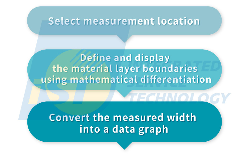
Figure 1: The auto metrology software is mainly divided into three steps.
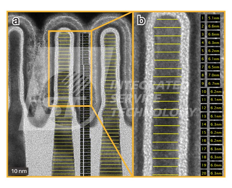
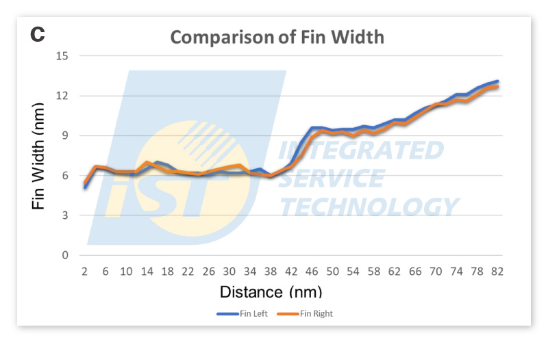
Figure 2: The result of the FinFET image displayed by TEM combined with the auto metrology software. (a) First, select the desired measurement location within the FinFET ; (b) It can be seen that the software can capture the Si Fin boundary every 2nm; (c) Statistical analysis of FinFET’s multiple line widths.
However, as the process continues to shrink down to 3 nanometers and even advances to 2 nanometer nodes, FinFET also begins to face physical limits such as leakage. Therefore, a new architecture called “Gate-All-Around FET” (GAAFET) has emerged. The GAAFET structure is divided into two forms: the first-generation nanowire (NW) and the second-generation nanosheet (NS). The difference between the GAAFET chip architecture and the FinFET includes the need to stack silicon (Si) and silicon germanium (SiGe) layers in nanosheet stack epitaxy. SiGe serves as a “sacrificial layer” in the subsequent “channel release.” SiGe is eaten away by etching to obtain a layer-by-layer nanowire or nanosheet, and then the nanosheet (wire) is covered with gate metal (High-k), as shown in Figure 3(a). Therefore, precise measurement of the SiGe and Si film thickness in GAA, as well as control of the SiGe shape, can accelerate the process improvement of GAA.
The newly introduced image auto metrology software in the iST Material Analysis Laboratory has three main functions:
- It can measure multiple layers at once and can set up to hundreds of measurement lines.
- The distance between measurement lines can be adjusted according to customer needs. For example, for measuring different layers of SiGe/Si, different distances can be set up as shown in Figure 3(b).
- It can provide customers with immediate measurement data. In the past, manual measurement could take up to an hour, but with this new auto metrology software assistance, it can be shortened to a few minutes.
As shown in Figure 3(b), this new auto metrology software can accurately capture the boundaries of each layer of SiGe and Si, allowing customers to know the remaining thickness of the SiGe layer after etching and adjust the etching parameters for different thicknesses. Therefore, it can accurately control the shape of the High-K after etching, and obtain a GAA structure with good uniformity and stability, which is also one of the most important factors affecting the performance of transistors.
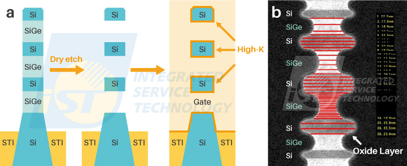
Figure 3(a): Simplified diagram of GAAFET fabrication process. Figure 3(b) shows the results of the GAAFET STEM image by using auto metrology software. The software can capture the boundaries of each SiGe and Si layer, and the spacing between measurement lines can also be customized.
Case Study 2: Quickly Obtain Meaningful Data Analysis for Nanoparticle Size and Distribution
Nanoparticles smaller than 100 nm are mainly used in catalysts, sensors, electrodes, and even in paint coatings. The iST Material Analysis Laboratory uses TEM combined with the latest image auto metrology software to accurately and quickly measure the size and shape of nanoparticles. After image processing, statistical data charts can be obtained to analyze the size and distribution of nanoparticles, and various values required in the development of materials at the same time, such as nanoparticle area, radius, particle average value, perimeter, etc., as shown in Figure 4(d), as a reference for the development of nanomaterials, shortening the development time.
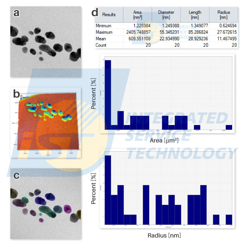
Figure 4: The result of the nanoparticle analysis showed by TEM combined with the auto metrology software. Figure 4(a) shows the TEM image of nanoparticles. From Figure 4(b), the software simulates a 3D topographic contour model. Figure 4(c) showed the nanoparticle image after image recognition by using the topographic contour model. Figure 4(d) showed the statistical data of the nanoparticle after image processing.
Case Study 3: Clear Identification of Grain Size Measurement and distribution
The number of grains per unit area is determined by the size of the grains, which has a decisive impact on material properties like hardness, tensile strength, toughness, and plasticity. Therefore, if the size of the grains in a material can be accurately measured, its material properties can be predicted in advance. Taking the example of the copper/titanium (Cu/Ti) layers in Under Bump Metallization (UBM), the iST Material Laboratory uses TEM combined with auto metrology software to clearly distinguish the shape and size of the grains from the Cu grain boundaries, as shown in Figure 5 below.
Furthermore, precise statistical results can be obtained for a large number of grains, as well as the various values required in material development, such as grain area, radius, particle average value, perimeter, and so on, as shown in Figure 5(b). The related values affect the electrical properties, hardness, diffusion, thermal migration, and other factors of UBM, helping customers to develop products more quickly in the new generation.
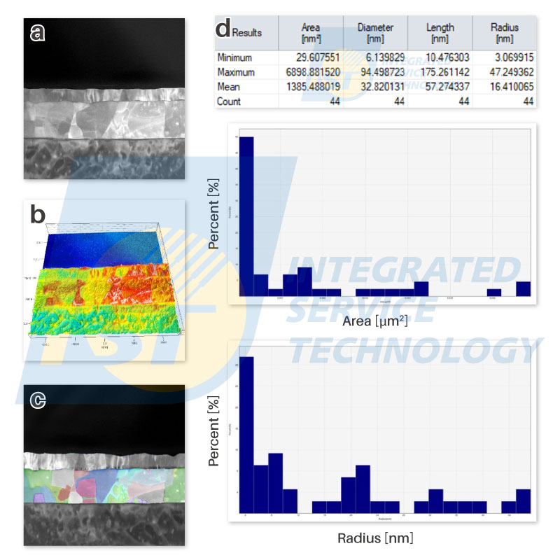
Figure 5: The measurement result of the UBM Cu/Ti layer showed by TEM combined with the auto metrology software. (a) STEM image of UBM grain; (b) the 3D morphology contour model simulated by the software; (c) the grain image after image recognition by using the morphology contour map; (d) showed the statistical data of the grain after image processing.
This is to share knowledge and experiences of iST with you. Should there be any inquiry or if you would like to know more about the aforementioned techniques, just ring Darry Chen at +886-3-579-9909 Ext. 6169 or email him at Tem_Tw@istgroup.com;marketing_tw@istgroup.com
References:
[1] 電子元件的靈魂-先進電晶體技術與發展趨勢| 劉致為教授
[2] K.S. Lee., et al. “Inner Spacer Engineering to Improve Mechanical Stability in Channel-Release Process of Nanosheet FETs. “June 2021; Electronics 10(12):1395.
[3] Loubet, N., et al. “Stacked nanosheet gate-all-around transistor to enable scaling beyond FinFET.” VLSI Technology, 2017 Symposium on. IEEE, 2017.
Other services you may be interested in
TEM Auto Metrology