Issued Date:2022/9/27 BGA Reverse
Issued By:iST
You may know that reverse engineering can help understand the design architecture of products to avoid patent disputes. Do you know when destructive sample delayering is unachieved, how to observe the sophisticated circuit layout through reverse analysis?
Among those unfamiliar with reverse engineering, it’s common to deem it the same as hacking, piracy, and only protects your own technologies from being used by competitors illegally but also prevents you from infringing the patents of your rivals.
Manufacturers in the semiconductor industry have been using reverse engineering as the main tool for IC R&D. The reverse engineering technique is assisting IC design houses in analyzing costs, man hours, talent, and technology required for new product development by extracting circuit to compare the latter against patent map databases, which is not only to evade the patented circuits of others but to get a better understanding of market status and exploitation of opportunities.
We have discussed reverse engineering issues in iST Classroom. We have reviewed how to observe the circuit layout of each die layer using delayering for nanoscale chips in advanced processes (Further reading: Delayer IC with this Method to Get the Entire Circuit Diagram Without Die Damage).
We have also shared how to see through the circuits in a nanoscale chip using large-scale scan and photography (Further reading: How to use SEM full-vision imaging technology to reverse-perceive nano-scale processing while avoid infringement?).
This month, let us show you how to extract layouts in a large scale in BGA package and even PCB through reverse analysis in the nanoscale work in terms of three examples.
BGA Reverse
Case 1: Extract circuits in all layers with 3D X-ray without delayering.
This example shows how to extract the layout of all layers in a BGA package. While removing the package with destructive pickling is impossible as it will damage the BGA structure, what should we do? The 3D X-ray is the solution. This is the non-destructive X-ray exposure technology for analyzing a secured device under test (DUT) at 360° together with a high-power optical lens. In this process, 2D images are extracted from different angles for the computer to reconstruct the DUT’s physical image.
It is special that we can extract different layers of the DUT to expose the internal structure. As shown in Figure 1, from the package to the die of a BGA DUT, the circuit of each layer can be extracted and displayed in images. We can also measure the width and pitch of the partial circuit, the size of vias, and the structural thickness of each layer.
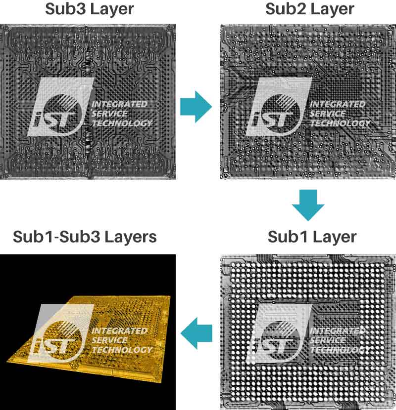
Figure 1: the images of each layer of a BGA substrate with the advanced 3D X-ray
Case 2: Getting a sharper image of circuit through delayering with grinding and OM photography
For small packages such as SiP and small BGAs, if the DUT is under 5mm*5mm and 3 layers, we can choose the non-destructive 3D X-ray reverse analysis. When the DUT is a large BGA sophisticated package with a size over 5mm*5mm, our failure analysis lab recommends delayering with backside grinding together with OM photography in order to get a sharper image of the circuit (Figure 2).
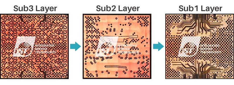
Figure 2: Images of different layers of a BGA substrate taken with OM photography after ordinary grinding.
Case 3: Two birds with one stone for the layout of both die and substrate circuits
In this example, besides extracting the circuit of the BGA substrate with reverse analysis, we also hope to analyze the metal layout of the die in the package, and even the overlapping of the substrate and metal layouts. So, can we analyze three layers (1–3) of the substrate with 3D X-ray first, then delayer the substrate with grinding and photograph the metal layer with OM, and finally overlap the images of layers 1–3 and the metal layer?
The answer is no! Because 3D X-ray and OM provide two different types of images that cannot be overlapped with one another. Additionally, when grinding the solder balls instead of the backside or front side of the IC, the sequence of photography and overlapping will be mirrored, making it difficult to judge (Figure 3 (left)).
What should we do then? iST’s failure analysis lab has developed an exclusive special reverse analysis method that can help you get the overlapping images of substrate layers 1–3 and the metal layer. With our exclusive image display software, you can overturn the images of each layer and overlay them from top to bottom (Figure 3 (right)) to facilitate circuit tracing and recognize the connection of each layer (Figure 4).
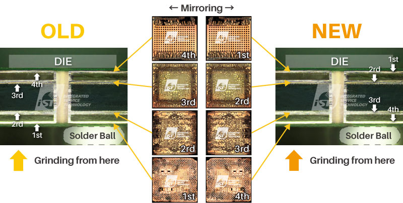
Figure 3 (left): When grinding the solder balls instead of the front-side of IC taking photography the sequence of photography and overlapping will be mirrored, making it difficult to judge.
Figure 3 (right): With iST’s exclusive image display software, you can overturn the images of each layer and overlay them from top to bottom.
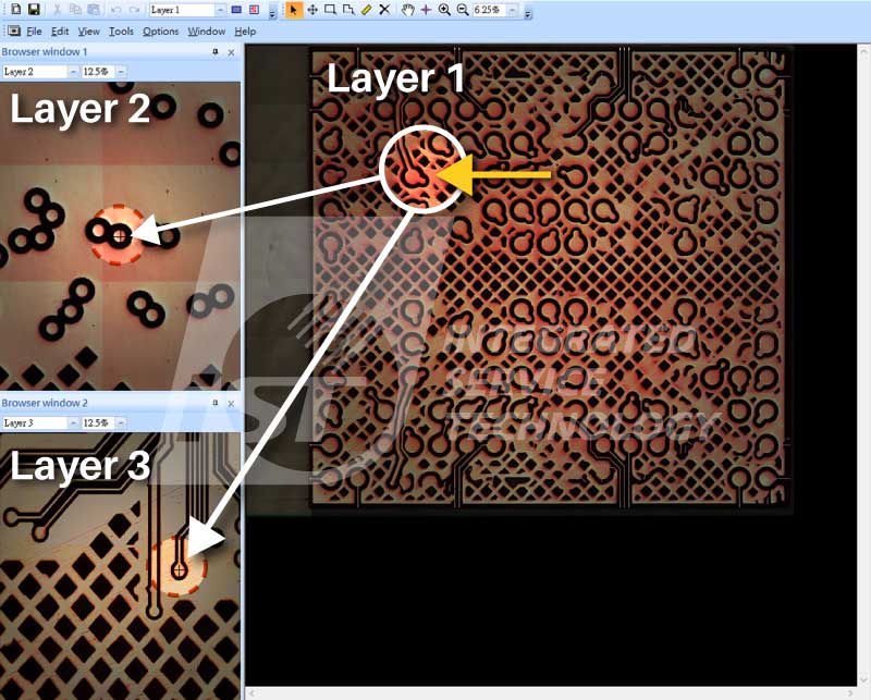
Figure 4: With iST’s exclusive image display software, users can trace the circuit and recognize the connection of each
For more information about reverse engineering to prevent patent disputes, please feel free to contact Ms. Chang at +886-3-579-9909 ext.6795 or Mr. Peng ext. 6762 by email to web_reverse@istgroup.com;marketing_tw@istgroup.com
Other services you may be interested in
BGA Reverse