Issued Date:2020/03/26Delayer
Issued By:iST
You may have learnt to prevent patent infringement by reverse engineering IC design.
However, it is technically difficult to extract the IC diagram completely by de-layering as chips get smaller. How to overcome it?
Delayer

Following Moore’s Law, the industry is pushing the process from 7nm to 5nm or even 3nm. This makes dies in ICs as tiny as ants’ eyes which are invisible to naked eyes. It’s very hard to retrieve circuits of each layer in dies by the ordinary IC delayering technique. In the worst case it may lead to not only poor yield, but also the complete loss of dies.
What else can we do to retrieve the entire circuit diagram to prevent patent infringement or debug the circuit of each layer?
Among those unfamiliar with reverse engineering, it’s common to deem it the same as hacking, piracy, and only protects your own technologies from being used by competitors illegally but also prevents you from infringing the patents of your rivals.
Manufacturers in the semiconductor industry have been using reverse engineering as the main tool for IC R&D. The reverse engineering technique is assisting IC design houses in analyzing costs, man hours, talent, and technology required for new product development by extracting circuit to compare the latter against patent map databases, which is not only to evade the patented circuits of others but to get a better understanding of market status and exploitation of opportunities.
Conventional die delayering skills may destroy or crack the samples as they are so tiny and ruin the subsequent process analysis operation. Without knowing circuits of the M1 (metal) layer, we can hardly learn about the memory block and get the circuit module analysis diagram.
This iST Tech Classroom program is to share with our long-time customers iST’s unique physical delayer skill. The latter delayers ICs, without the package removed, by magnifying the samples to not only improve engineering yield but also retrieve the entire circuit diagram. In addition, the same skill may get applied in cases of alloy PAD, precision ICs, and other IC samples which cannot retrieve the die, yet require delayering.
Three Steps: IC delayer, prevent damaging dies, retrieve entire circuit diagram
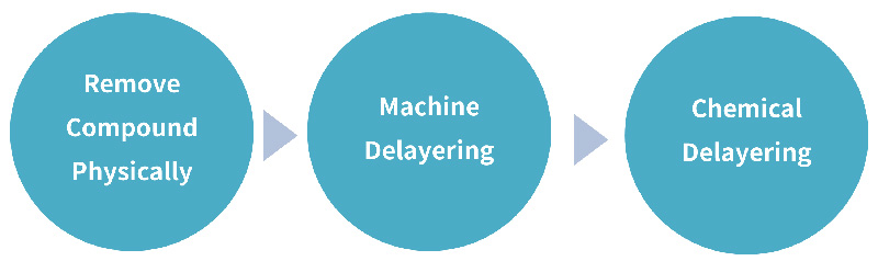
Figure 1: Retrieve entire circuit diagram with the iST exclusive three steps
Step 1: Ready the Sample by Removing its Compound Physically
Physically remove remaining compound on the front of the die while the IC package remains existed. Differing from conventional delayering on package removed dies, this method can not only apply to samples of larger area/volume, but can also suffer fewer lost dies in later delayering operations while maintaining flat die surface (figure 2).
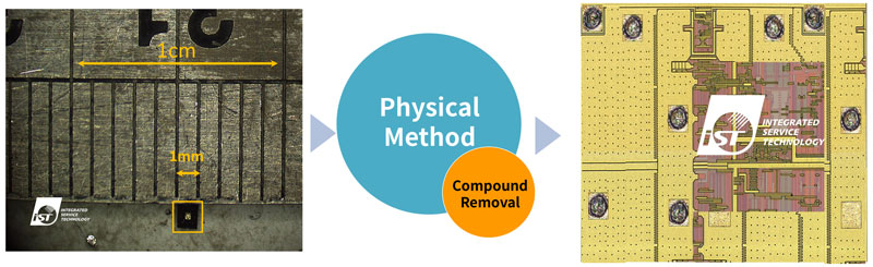
Figure 2: ICs of advanced process are very tiny. Addressing this, iST removes the sample’s compound physically to retrieve the circuit diagram of the top layer
Step 2: Machine Delayering
Etch off the non-target area of IC passivation and oxide with an ion etching machine at required settings through iST’s exclusive parameters to keep lower metal layers intact (figure 3).
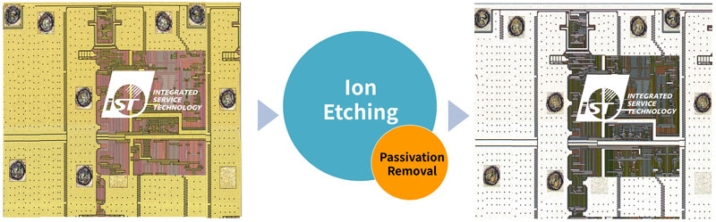
Figure 3: Remove the protection layer with plasma ions (step 2)
Step 3: Chemical Delayering
Once the passivation gets removed, soak area needing to be removed in the metal layer with chemicals to retrieve the entire circuit diagram.
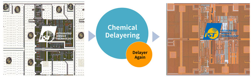
Figure 4: Soak to remove the metal layer with chemicals once the passivation gets removed to retrieve the entire circuit diagram
Should you have any inquiries for delayering methods or any further requirements, just ring Mr. Su at +886-3-579-9909 EXT 6739 or email us at ca@istgroup.com