Issued Date:2022/6/28advanced packaging joint defect
Issued By:iST宜特
When the board level reliability (BLR) test fails and you are asked to debug, how to quickly find the defect locations in 3 simple steps?

The board level reliability (BLR) test is a common method used to verify solder joint strength across the globe. By simulating components on the PCB, we can re-present the potential soldering problems of solder balls. (Further reading: What does BLR mean for IC Design Engineers?)
In the first step of BLR, it is necessary to make a daisy chain design to form a network of all solder joints connecting the components and the PCB to monitor the yield of each solder joint in real time. With this test, we can find out if the solder ball on each solder joint is defective and even accurately capture the failure time and make early improvements.
advanced packaging joint defect
advanced packaging joint defect
A daisy chain circuit can be divided into two parts, one on the IC and another one on the PCB test board. When mounting the IC on the PCB with surface mounting (SMT), a complete daisy chain is formed.
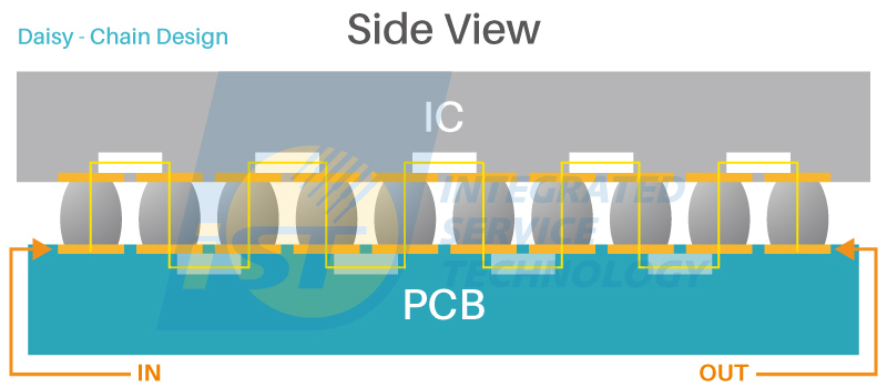
Figure 1: Illustration of a daisy chain design
However, when the result is a failure after a series of BLR tests, how do analyze failures to find the causes of impedance change?
In this session of iST Classroom, we will share two examples with you: ordinary packaging joint defect and advanced packaging joint defect. We will show you how iST Lab helps you debug, clarify the causes, make quick corrections, and run re-verification to ensure timely product launch in 3 simple steps: location navigation, assistant imaging, and slicing (Figure 2).
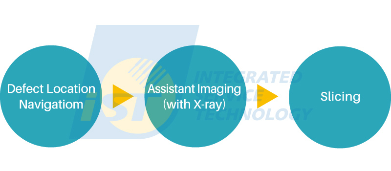
Figure 2: Finding anomalies with 3 steps: location navigation, imaging, and slicing.
1. Ordinary packaging: Running interconnect electrical tests with the bisection method
If leakage or short happens after the BLR test, iST Lab will: (1) navigate the coordinate (X, Y) of failure points with the hot spot testing machine, such as Thermal EMMI (InSb); (2) run non-destructive X-Ray/3D X-Ray imaging; and (3) slice the fail section and analyze the root cause using low-stress Plasma-FIB or cross-section polish with the scanning electron microscope (SEM). (Further reading: Determining Whether IC Defects are Caused by the Poor Packaging)
If “open circuit” happens after BLR tests, it will be impossible to find the abnormal location with hot spot analysis because current cannot pass through the circuit. Hence, before running step 1—location navigation, it is necessary to prepare the sample with destructive cross-section polish from the PCB test board to expose the daisy chain interconnections (Figure 3). Then, use the electrical test with the bisection method (Figure 4) to find the relevant abnormal positions (locations).
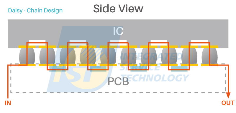
Figure 3: Cross-section polished the PCB to expose the daisy chain traces.
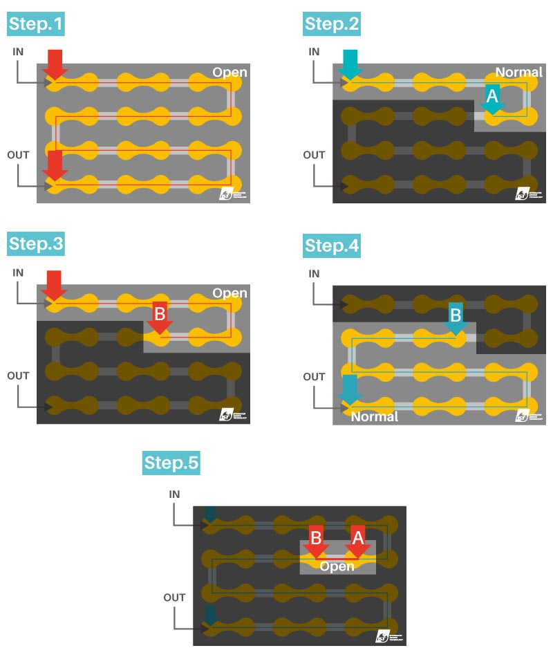
Figure 4: Use the electrical test with the bisection method to progressively find the relative anomaly positions. First, charge IN and OUT (Figure 4 (1)), the circuit is open (anomaly). Next, charge IN and A (Figure 4 (2)), the circuit is normal. Then, charge IN and B (Figure 4 (3)), the circuit is open (anomaly). Also, charge OUT and B, the circuit is normal. Lastly, charge B and A (Figure 4 (5)), the circuit is open (anomaly). With the bisection method, the relevant anomaly positions are located.
Step 2, by imaging abnormal points with X-ray, as shown in Figure 5 (left), we can clearly see the anomaly (imaging) between the solder ball and solder pad. Step 3, by slicing the PCB (slicing), as shown in Figure 5 (right), we can see that the solder ball crack, causing the impedance abnormal.
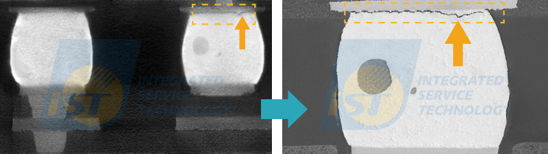
Figure 5 (left): An anomaly between the solder ball and solder pad. Figure 5 (right) Solder ball crack is detected by slicing.
2. Advanced packaging joint defect: Finding anomalies with EBAC
While advanced packaging is used on multiple dies, e.g. 2.5D or 3D ICs, the daisy chain design will be different from the ordinary single test board for single die design. Instead, multiple dies are packaged on one single test board (Figure 6). In this case, how to find the abnormal points after failing the BLR tests?
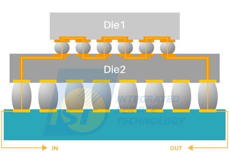
Figure 6: The daisy chain interconnection of advanced packaging.
If short or leakage happens after BLR tests, the same electrical failure analysis for ordinary packaging can be used. First, use the hot spot test with Thermal EMMI (InSb) to locate the anomaly position and then X-Ray/3D X-Ray imaging. Lastly, slice the failure section with Plasma FIB or cross section polish.
If “open circuit” happens after BLR tests, follow the instructions as for ordinary packaging: prepare the sample before “location navigation.” However, the daisy chain interconnections of ordinary packaging are between the IC and PCB (see Figure 7 (left)). In advanced packaging, the daisy chain interconnections are between two dies (Figure 7 (right)). Hence, instead of the traditional cross-section polish from the PCB (no interconnections on the PCB), it is necessary to remove silicon on the backside of the dies by using dry etching (Further reading: Identify Solder Ball Defect in Advanced Packaging from Die Backside) to expose the daisy chain interconnections between dies 1 and 2.
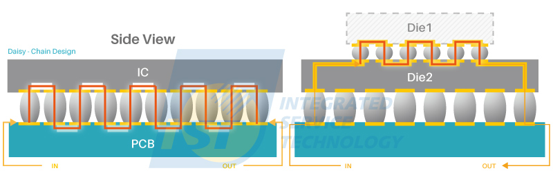
Figure 7 (left): In ordinary packaging, the daisy chain interconnections are between the PCB and IC. Figure 7 (right): In advanced packaging, the daisy chain interconnections are between dies 1 and 2. Use dry etching to expose the daily chain interconnections in die 1.
After exposing the daisy chain interconnections (Figure 8 (right)), step 1 (location navigation) could be continued. However, if the circuit is open and current cannot pass through, it will be impossible to detect the hot spot location using Thermal EMMI (InSb). Then, electron beam absorbed current (EBAC) should be used to charge electrons on the sample. As charge will only accumulate at the normal interconnections, locations with abnormal charge will be dimmed, i.e. we can convergence abnormal location (Figure 8 (right)).
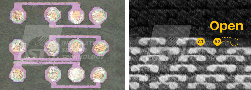
Figure 8 (left): Observe the exposed daisy chain interconnections in the prepared sample with OM. Figure 8(right): The abnormal locations could be judged while the interconnection between A1 and A2 is dimmed as shown with EBAC.
In step 2 imaging, X-ray or 3D X-ray is arranged for the re-examination, showing the bonding anomaly of solder balls (Figure 9 (left)). In step 3 slicing, Plasma FIB or cross-section polish is arranged to inspect the sample’s cross section view, showing that non-wetting phenomenon on the solder joint is the cause of anomaly (Figure 9 (right)).
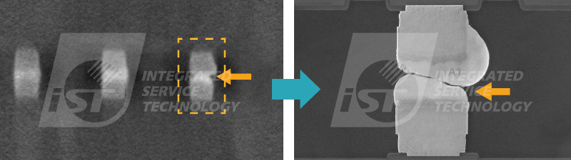
Figure 9 (left): X-ray imaging shows that bonding anomaly of solder balls.
Figure 9 (right): Slicing imaging verifies that non-wetting phenomenon on the solder joint non wetting is the cause of anomaly.
This article is aimed to share our experiences with honorable clients like you. In case you want to know more details, please call Mr. Emily Yang at +886-3-579-9909 Ext. 6757 or email: web_ise@istgroup.com, marketing_tw@istgroup.com
Other services you may be interested in
advanced-packaging-joint-defect