Issued Date:2021/4/7IC Quick Assembly
Issued By:iST
Due to the over-demand situation of assembling, new product development is now being delayed as OSATS’ existing capacity is too stretched to provide engineering samples assembling required by IC R&D. How to deal with this dilemma?
IC Quick Assembly
Fast spreading of the COVID-19 pandemic in 2020 has been outrunning the bonding and packaging industry capacity with booming conventional packaging demands. This is especially the case of IC demands for PC/NB, their peripherals and consumer electronics driven by the trend of work from home (WFH) and QFN packaging required by reliability-focused automotive electronics.
Traditional large-scale OSATS (Outsourced Semiconductor Assembly And Test) are confronted by over-capacity demands in Q1 2021 or through to the end of June. As these houses show no signs of adding capacities in meaningful amounts, the delivery of IC designs had been bottlenecked, let alone making engineering samples required by new products R&D.
Generally speaking, IC design houses at the R&D stage must package their pilot-run wafers and chips before doing any engineering verification.IC Quick Assembly
iST has been experiencing increasingly needs for engineering samples’ quick assembly before clients are seeking for engineering verification by iST in recent days. Drilling down, we found that when leading OSATs are deluged with the demands for mass production, these non-recurring engineering (NRE) packaging and relatively few samples for verification required by IC design houses are doomed to be held off again and again.
The iST’s quick assembly lab has been packaging and bonding hundreds of thousands engineering sample ICs for clients annually since its foundation more than two decades ago. This iST classroom is presenting you with the steps taken by iST’s quick assembly lab to deliver your packaging samples in only a couple of hours. In addition, iST is offering solutions to remove the bottleneck in testing special chip samples’ packaging and enable their later measurement successfully.IC Quick Assembly
1. Ordinary Chip Sample Packaging: Get Engineering Samples Packaged with Ceramic Materials in Six Hours
Chips by mass production are conventionally packaged with a lead frame and the substrate by a process with 20-30 steps lasting 3-10 days. The iST’s quick assembly lab has simplified this process to just 4 steps (Figure 3) through the ceramic (Figure 1) and plastic pre-mold (Figure 2) and reference PCB provided.
First of all, validate the wire bonding diagram: you may provide iST with the diagram by the assembly house or have iST prepare it and select the materials needed based on chip data you provided. iST will start making official samples once the layout gets validated. The next step is to mount dies on packaging materials with conductive or non-conductive adhesive before bonding them with the required wires and given wire diameter per specifications of the chip.
Addressing customer’s test or use methods, iST may deliver the packaging samples for engineering verification in just 6 hours with the chip and wire protection glass or ceramic cap or sealants provided by iST.
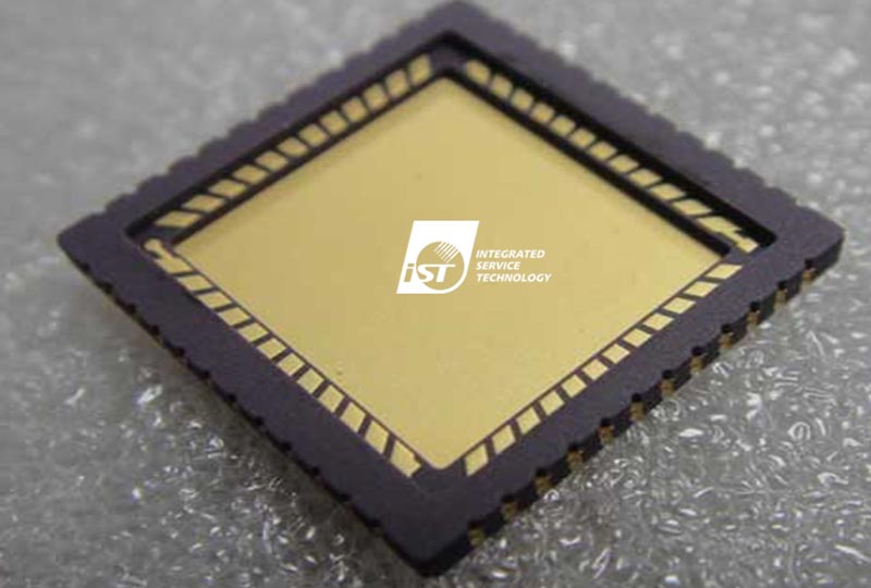
Figure 1: Ceramic substrate
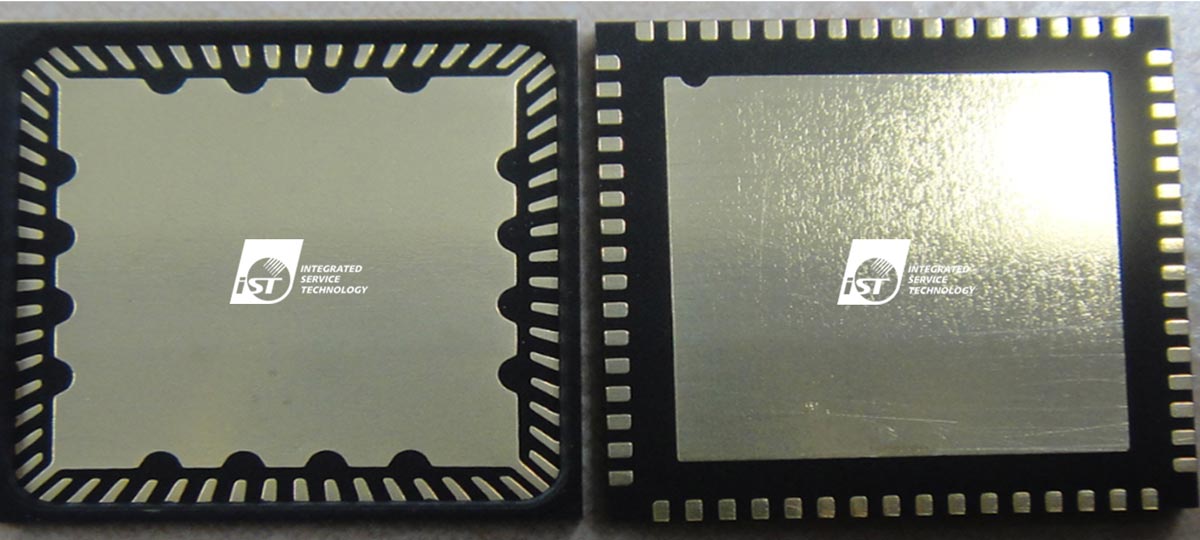
Figure 2: QFN packaged with plastic pre-mold
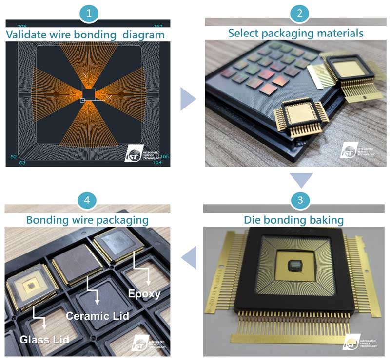
Figure 3: Quick assembly in just 4 steps
2. Special Chip Packaging Sample: How to Test the Electric Characteristics for Non-Ordinary Measurement Requirements?
IC design engineers may test post-packaging samples sent back by iST to identify design anomalies. They may have to test special signals yet the original packaging does not provide the required data. In cases like this, what can we do about it?
Case 1: Shape up wire route (Figure 4) with FIB circuit editing microscope, i.e., built up conduction bore and solder pad with focused ion beam then connect the pad to a metal bridge with a special bonding mechanism, to enable the clients’ subsequent measurement operations.IC Quick Assembly
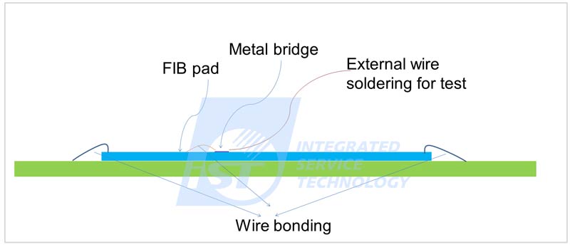
Figure 4: Build up route of wire with iST’s N-FIB
Case 2: Client provides verification required non-wire bonding chip. Either solder bump or copper pillar, iST enables fast wire bonding for the client’s verification later (Figure 5).
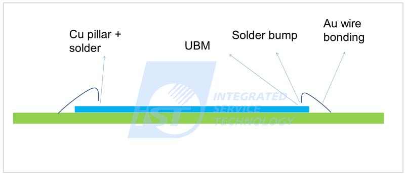
Figure 5: iST’s quick assembling lab may lead signals of dies with metallic wires, based on special wire bonding parameters, for the engineer’s follow-up testing.
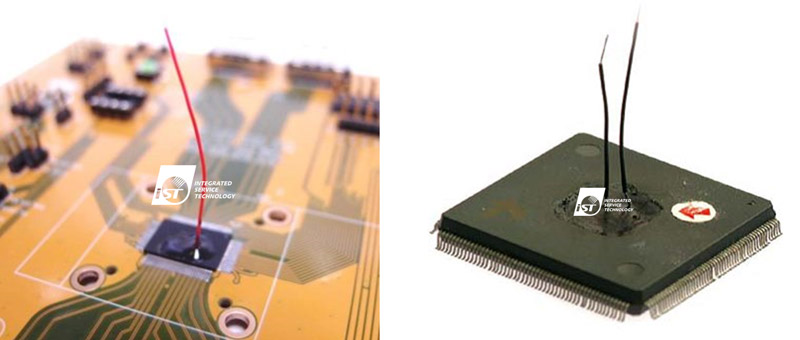
Figure 6: Lead signal out of chip

This is to share knowledge and experiences of iST with you. In addition to quick assembling, iST lab provides services for wafer sawing, die attaching, wire bonding, etc. An One-stop Solution based flip chip packaging service aligned with your chips and tailor-made substrate also provided for you to enable ESD, OLT and reliability analysis and shorten the preparation time of samples under test effectively. Should there be any inquiry or if you would like to know more about the aforementioned techniques, just ring Mr. Peter Chen at +886-3-579-9909 Ext. 6861 or email him at ist_assy@istgroup.com.