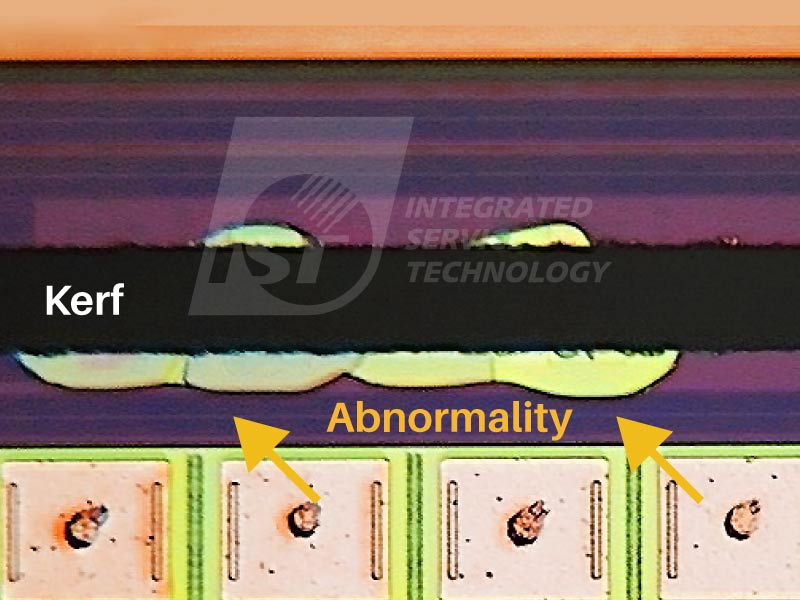
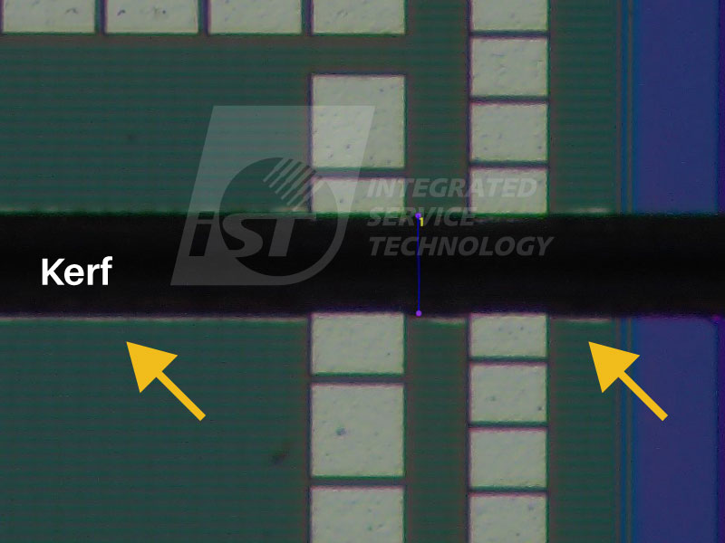
The Superiority of iST
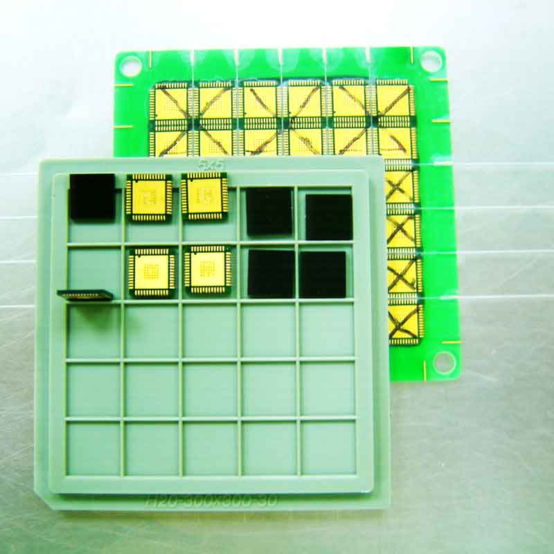
In addition to internal dicing machine for wafer of size up to 12″, iST provides one-stop high-quality solutions from sample dicing, wire bonding, ceramic packaging, to COB packaging. All these are designed to cut test sample preparation time effectively.
Case Sharing
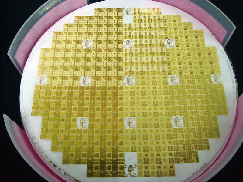
- Ordinary wafer dicing
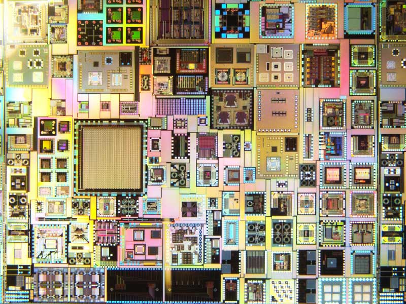
- Multi-chip wafer dicing
- Shared chip re-dicing
- Substrate dicing (with or without adhesive)
- Ceramic/glass board dicing
- IPD dicing
- Multi stacker wafer
- Narrow kerf width
- High density wafer
Contact Window | Mr. Yang/Benson | Tel:+886-3-5799909#6862 | Email: web_ass@istgroup.com

