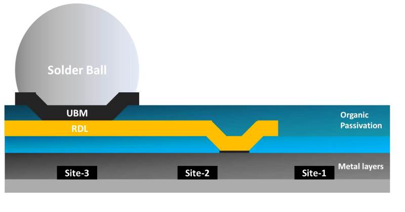
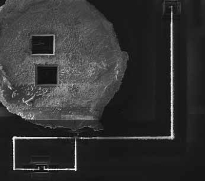
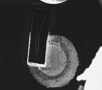
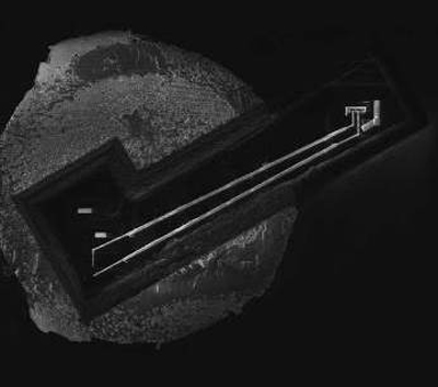
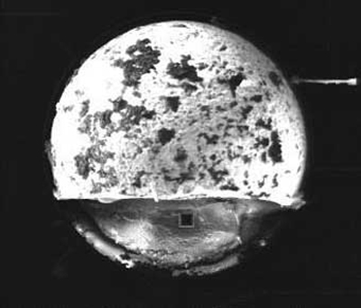
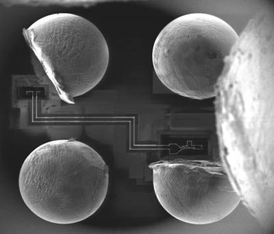
IC products packaged with WLCSP (Wafer-level chip scale package) are confronted with two big challenges in FIB circuit edit. Most parts of circuits of an IC are covered by the bumps and the RDLs (redistribution layer) and cannot be edited. Even if there are circuits not covered by the bumps and RDLs, as the organic passivation on top is thicker, greater effort and more time is needed to edit these circuits.
The Superiority of iST
Case Sharing
Contact Window | Mr. Wang/Chino | Tel: +886-3-5799909#6000 | Email: web_fib@istgroup.com


