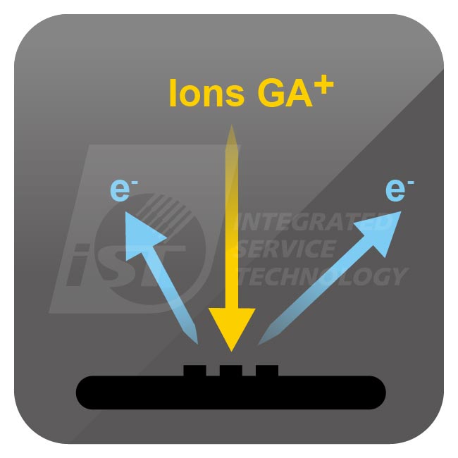
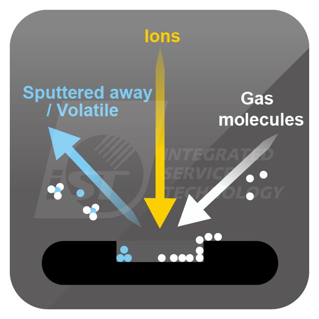
Etching mechanism
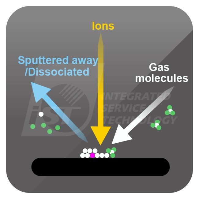
Deposition mechanism
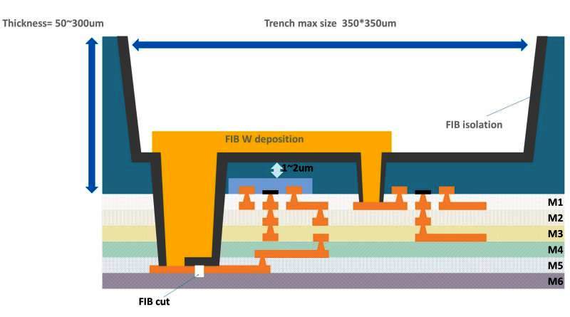
The focus ion beam (FIB) technique may selectively etch (disconnect circuit) and deposit conductor or nonconductor (add new circuit) by hitting sample surface with gallium ion along with organic gas.
What iST can do for you
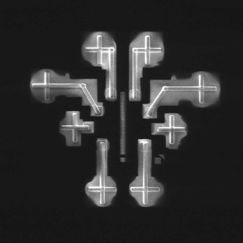
FIB circuit:
IC circuit edit is provided to the designers through FIB. Due to the merit of saving a photo mask redo, FIB significantly shortens time for IC prototype validation and time-to-market.
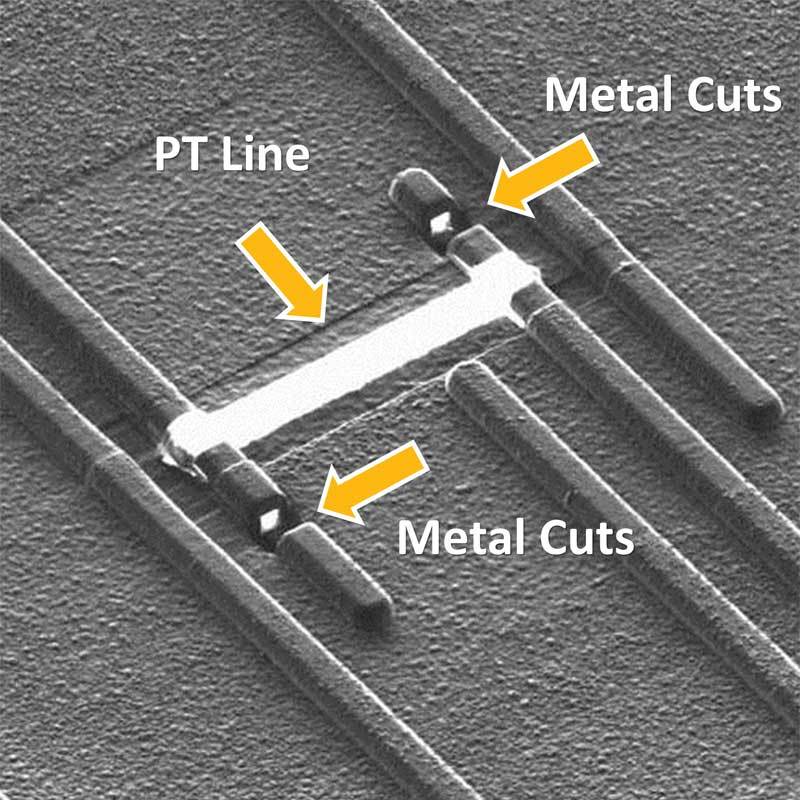
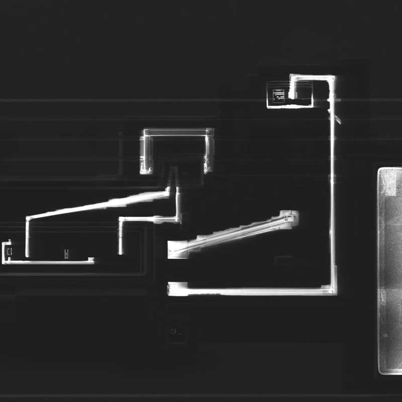
CAD Probe Pad:
Using FIB, points where signals must be measured are led to the surface of the IC so that a mechanical prober may retrieve internal signals in IC.
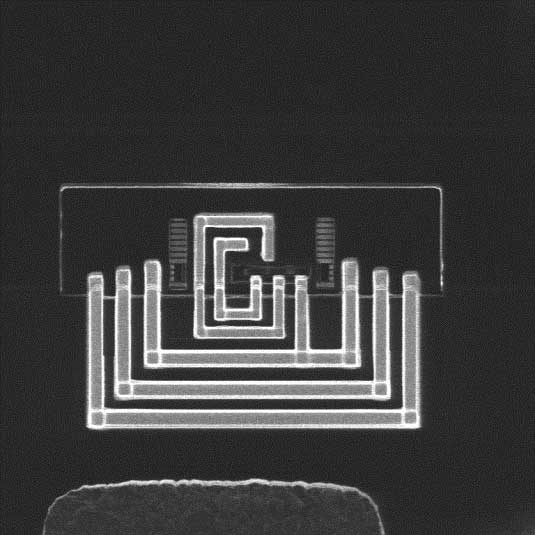
Backside FIB Circuit Edit:
Modifying circuit from backside may have better feasibility and success rate amid limited flip-chip packaging substrate, advanced process continuously edging into 3nm, increasing metal winding layers, and still more complex and tighter circuit

The Superiority of iST
Case Sharing
- Minimum Operation On 3nm Process Metal With 3.5nm Resolution.
- Maximum applicable to 8” wafers.
- Support CAD Navigation.
- Precision laser guided stage.
- Built-in infrared microscope for observing CMP layer and isolating silicon layer.
- Two choices for metal wires: tungsten (low resistance) or platinum (faster).
- Build with FEI DE/DX etching gas so as to increase the yield rate when apply to high aspect ratio and tighter circuit layout.
| Model | Capability Process | Capability Note |
|---|---|---|
| Centrios | 5nm |
|
| V400ACE | 7/16/22nm |
|
| 986-IET | 40/65nm |
|
| V600CE | 90/110nm |
|
| V600 | ≧130nm |
|
- Before FIB, test once more after decapsulation, wire bonding or packaging.
- Yield decreases if multiple modifications are made on the same IC.
- The resistance of conductor metal by FIB is higher than the original. Any low resistance conductor demand, please specify it on the service order.
- Suggest providing GDSII circuit layout to facilitate navigation (partial area or layer will be fine), this can help increase the yield.
Contact Window | Mr. Wang/Chino | Tel: +886-3-5799909#6000 | Email: web_fib@istgroup.com