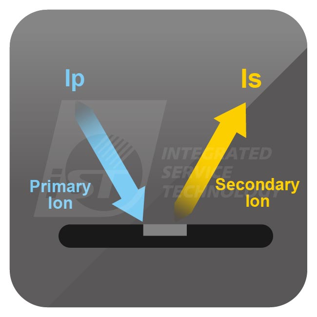
Secondary Ion Mass Spectrometer (SIMS ), this mechanism executes quantitative analysis over micro contamination, doping, and ion implantation as well as junction diffusion behavior study with high resolution detection capacity based on the high sensitivity of ions. This makes it ideal for trace detection and analysis over semiconductor, LED and thin film material detection and analysis.
The Superiority of iST
Case Sharing
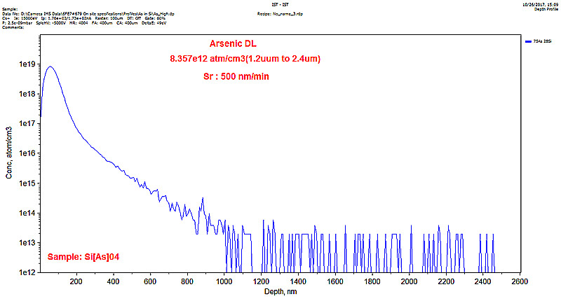
Analysis sample: semiconductor silicon wafer
See the chart below for the highest limit of iST SIMS device in terms of implanting concentration of arsenic (As) ions in semiconductor silicon wafer is analyzed. It tells the detection limit of SIMS may reach up to 0.2 ppba.
Depth profiling of As ions (N type) implanted in Si chips
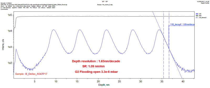
Analysis sample: semiconductor silicon wafer
Find out SIMS depth resolution with multi-layers of nano-thick boron (B) implant analysis. The minimum depth resolution of depth profile analysis featured by iST SIMS device based on this special high-resolution analysis technology is 1.65nm.
Depth profiling of B ions (P type) implanted in Si chips
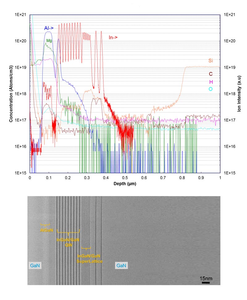
Analysis sample: LED epitaxial
LEDs samples usually need to observe 7 or 8 trace elements during SIMS analysis. Figures below tell concentration profile of Mg (P type) and Si (N type) in epitaxial; combining with the TEM analysis and relative position of elements in epitaxial can be identified.
Upper figure: identify concentration distribution through SIMS analysis
Lower figure: identify relative position of elements through TEM analysis
- Detection limit: up to ppma(1E-6) or even ppba (1E-9)
- Capable of detecting all elements in the periodic table (H~U)
- Capable of distinguishing between isotopes
- Depth resolution: up to 2nm
- Capable of analyzing samples of poor conductivity
- Capable of quantitative analysis by comparing against standard unit
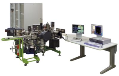
CAMECA 6F-E7
| Source of ion | Cs: 2~10kV O2: 1.1~15kV |
| Detection limit | ppma ~ ppba |
| Detectable elements | H~U |
| Mass resolving | >20,000 |
| Analysis area | >10um |
- Semiconductor Industry
- LED Industry
- Optoelectronics Industry
- PCB Industry
Contact Window | Mr. Chang /Johnson | Tel:+886-3-5799909#6613 | Email: sa_tw@istgroup.com

