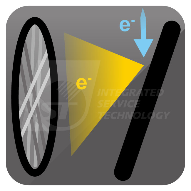
Electron Backscatter Diffraction (EBSD) is a non-destructive analytical technique commonly used in electron microscopy (EM). When a high-energy electron beam interacts with a sample’s crystal lattice, it produces characteristic Kikuchi patterns. By comparing these patterns with a reference database, researchers can identify various microstructural features of the crystal, including grain size, lattice characteristics, grain boundaries, crystallographic texture, and strain
What iST can do for you?
EBSD (Electron Backscatter Diffraction) is a powerful technique for studying the microstructure of crystalline materials. By using EBSD, we can help clients analyze critical grain-related properties—such as grain size, morphology, distribution, and orientation—as well as perform crystal phase identification, texture (preferred orientation) analysis, and grain boundary characterization. These insights enable customers to optimize material selection and improve manufacturing processes.

The Superiority of iST
Case Sharing
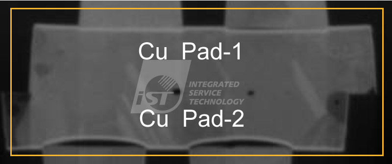
A hybrid bonding structure undergoes recrystallization during bonding under specific temperature and pressure conditions.
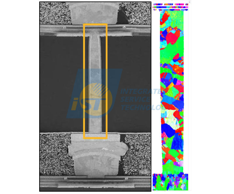
Grain orientation distribution within a TSV of advanced package product
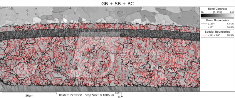
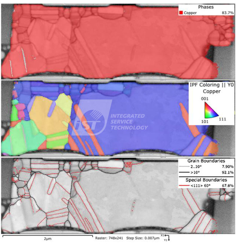
Grain and grain boundary distribution map of a copper pillar
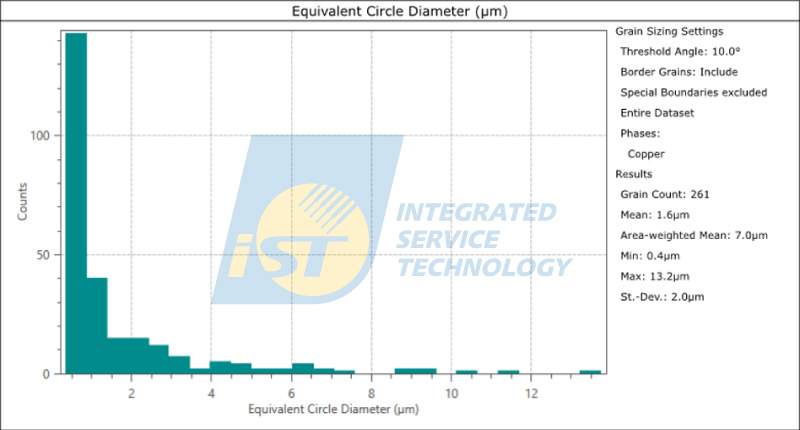
Statistical table of copper pillar grain sizes
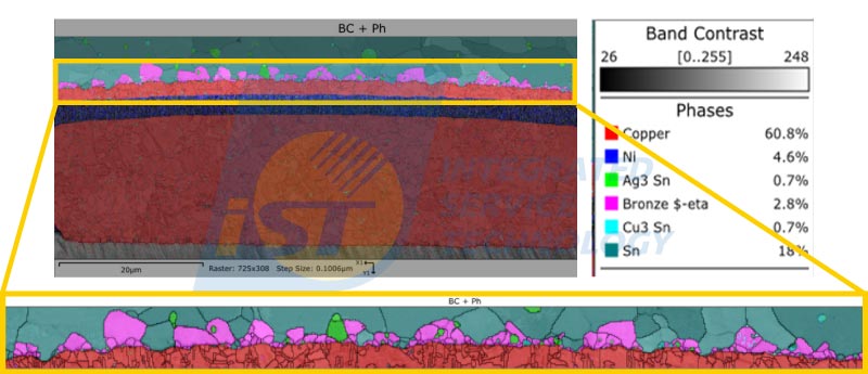
Phase distribution map of a copper pillar
Phase identification and distribution in a Cast Iron
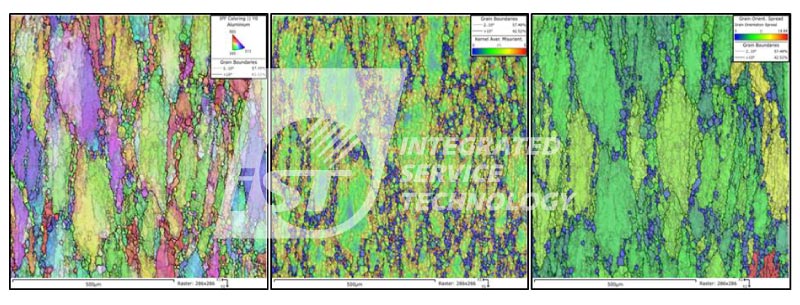
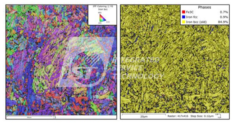
Lattice and strain distribution in a rolled aluminum
- Semiconductors: IC manufacturing process, advanced package
- Metals & Alloys: copper, iron, aluminum, nickel metals/alloys, etc.
- Intermetallic Compounds (IMCs): copper-based, nickel-based, titanium-based, etc.
- Ceramics: ITO, alumina (Al2O3), zirconia (ZrO2), SiC, WC, etc.
- Thin Films: crystalline coatings
- Minerals
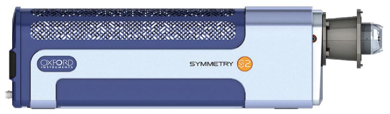
Oxford Symmetry EBSD Detector
| Detection Limit | rain size>20nm |
|---|---|
| High Speed (pps) | 4500 |
| High Resolution (pixels) | 1244x1024 |
| High Angular resolution (Deg.) | 0.05. |
- Semiconductor
- Metalwork
- Aerospace: aluminum components, blades, valves, etc.
- Automotive: blades, valves, etc.
- Earth Sciences
Contact Window | Dr. Lin, Wei-jui | Tel:+886-3-5799909#6166 | Email: web_ma@istgroup.com