Issued Date: 2018/12/13
Issued By: iST
Why is FSM needed?
Why is FSM needed only for some wafers?
Which two options are available for FSM?
1. Why is FSM needed?
FSM is a critical process for MOSFET wafer thinning. Featuring high switch speed, low input impedance and low power consumption, the MOSFET is required to stand large current. In terms of process it requires a clip bond expanded current path to replace the wire bond for lower wire resistance and RDS (on) (drain-source on resistance).
The FSM process is aimed to form UBM by sputtering deposition orElectro-less Plating, followed with clip bond soldering to reduce wire resistance.
In case of clip bond soldering, an Under Bump Metallurgy (UBM) solder surface in between the Al pad and clip is required. The UBM is composed of different metallic elements, for sputtering deposition is Ti/NiV/Ag and for Electro-less Plating is NiAu/NiPdAu.
2. Why is FSM needed only for some wafers and which ones require it?
For MOSFET components to undergo clip bond or mixed bond (source goes with clip bond and gate with wire bond), they need a layer of UBM atop Al pad to connect to clip. That is, MOSFET components without large current applications can have a direct wire bond on the Al pad and end up without FSM.
3. Options available to car electronics and advanced application – sputtering deposition
The sputtering deposition process can be outlined in the following steps: 1. Deposit Ti/NiV/Ag layer on wafer with high vacuum sputter machine; 2. Coat photoresist; 3. Expose and development with photomask (photo lithography); 4. Shield the Al pad upper surface before etching away excess UBM (etching process). This is a mature, stable, and extremely reliable and has long been adopted by many car electronics and high-end application manufacturers.
Typical Sputtering Deposition Process
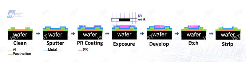
Figure 1: The sputtering deposition process needs multiple machines and process including metallic sputtering, photo resistance coating and development, wet etching, and photo resistance removal.
4. The high CP alternative of MOSFET FSM process – Electro-less Plating
The aforementioned sputtering deposition process is mature and stable at higher production costs and longer production time due to multiple processes employed (including high vacuum sputtering, photo lithography, and etching). This, inevitably, sets back certain more cost sensitive MOSFET components makers.
iST, your long-term partner caring about your concerns and requirements, has come up with an alternative: the “redox reaction” based Electro-less Plating.
Also known as chemical plating, the electro-less plating employs a series of chemicals-based controllable redox reactions to deposit a layer of film of metallic ions atop a wafer surface without any help of external current.
The most important feature of Electro-less Plating is to selectively deposit nickel-gold/nickel-palladium gold on the Al pad by a series of redox reactions without high vacuum sputtering, photo lithography, and etching. This not only cuts costs but also reduces production time.
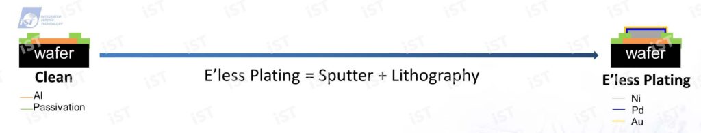
Electro-less Plating Process

Figure 2: The Electro-less Plating process mandates just one machine to execute a series of Electro-less Plating steps; relative to multi-steps required by sputtering deposition, the Electro-less Plating gives the same results at a relatively simpler process.
5. Production Flow of Electro-less Plating
The production flow of Electro-less Plating: inspect surface of wafer, put cassette in the wafer load port of machine, read bar code, auto load the recipe required for making the batch from the Manufacturing Execution System (MES), run the recipe automatically, after the process ended, the system prompts operators to remove finished wafers out of the unload port. This seemingly simple production flow is actually composed of a comprehensive chemical reaction under precise control.
As illustrated in Figure 3, the Electro-less Plating process begins with pretreatment and is followed by the first zinc activation (Zincation), the removal of coarser zinc activated particles with nitric acid (HNO3), the second zinc activation to form finer zinc activated particles, and then ends with NiAu/NiPdAu deposition.

Figure 3: Electro-less plating flow chart
6. Sputtering Deposition V.S. Electro-less Plating
In case your products require FSM process for manufacturing and you are focusing on high capability/price value and optimum costs, Electro-less Plating is a good choice as it can deposit NiPdAu film on Al pads and is suitable for clip bond; on the other hand, if you are aiming at high quality and reliability, then choose sputtering deposition for its excellent reliability with high vacuum metal sputtering and photo resistance designed pattern.
Table 1: Electro-less plating V.S. Sputtering deposition
Electro-less Plating Sputtering Deposition Mechanism Redox reaction Physical gas phase deposition Pattern formation Selective deposition Requires photo lithography and etching process Metal NiPdAu or NiAu Ti/NiV/Ag Cost Lower Normal Reliability Acceptable Excellent Production time Short Normal (including photo lithography)
This article is aimed to share our experiences with honorable clients like you. In case you want to know more details, please call Mr. Yu(Stan) at +886-3-579-9909 Ext. 5888 or email: web_sp@istgroup.com.