Issued Date:2024/8/1 SRAM Failure Analysis
Issued By:iST
Static Random-Access Memory (SRAM), known for its high-speed operation, low latency, and low power consumption, is essential for the logic IC products including high-performance computing (HPC) and machine learning tasks required in artificial intelligence (AI) applications. However, when SRAM malfunctions, identifying the root cause of the failure becomes challenging due to the dense and repetitive structure of SRAM cells.
SRAM Failure Analysis

Memory devices are categorized into two types: non-volatile and volatile memory. Non-volatile memory, which is used for long-term storage, retains data even when power is off, such as Flash memory. On the contrary, volatile memory temporarily stores data for high-speed computation under chip power-on condition. The key difference between non-volatile and volatile memory therefore can be distinguished by that the stored data is retained or not after system is power-off; when power is off; volatile memory loses data, while non-volatile memory retains it.
As described in previous paragraph, both SRAM and DRAM are volatile memory types. As long as power is supplied, the information remains intact; once system power is off, the data cannot be retained thereafter.
Compared to DRAM (store information by pumping charges), SRAM does not require periodic refreshing of data to retain the information, which is making it more energy-efficient and faster in memory operation. Besides, the SRAM structure is easier to be integrated with typical process of logic products. The benefits from both performance and high manufacturing compatibility make SRAM as the preferred choice for cache memory in CPUs and GPUs.
At the 2022 International Electron Devices Meeting (IEDM), TSMC highlighted that the SRAM cells in its 3nm (N3) process is reduced by only about 5% compared to the 5nm (N5) process. Similarly, Intel’s SRAM density in the Intel 4 process shows only a 23% reduction compared to Intel 7. Despite these SRAM scaling challenges in advanced nodes, SRAM technology remains critical for advanced applications in AI and high-performance computing (HPC).
To meet higher performance and power efficiency demands in advanced chips, design teams are exploring methods to enhance CPU performance, with SRAM stacking on top of CPUs as one approach to achieve optimized power, performance, and area (PPA) metrics. To analyze failures in densely packed and repetitive SRAM structures within ICs is very important for enhancing chip yield and product stability. In this episode of iST’s classroom, we provide insights into SRAM operation principles, common SRAM failure modes, and employs FA techniques to identify root causes of defects.
SRAM Failure Analysis
SRAM Failure Analysis
1. SRAM Read/Write Mechanism
A SRAM cell can be composed of six (6T), eight (8T), or ten (10T) transistors. Certain SRAM cells even provide multi-port read/write functions. 6T SRAM is the most common structure for such volatile memory. A 6T SRAM cell comprises two PMOS transistors (Pull-Up (PU) devices) and four NMOS transistors (2 Pull Down (PD) devices and 2 Pass Gate (PG) devices). Each paired PU and PD form as an inverter and the 4 devices (2PUs and 2PDs) are designed to connected as a latch circuit to retain the stored data. The PU transistors (Load Transistors) maintain high voltage states (logic 1), while the PD transistors (Drive Transistors) maintain low voltage states (logic 0). The PG transistors (Access Transistors) facilitate data read/write operations by connecting to the bit lines (BL). In a single bit, the high and low voltages of the two nodes (Q and Q) are interchanged to represent the binary states 0 and 1.
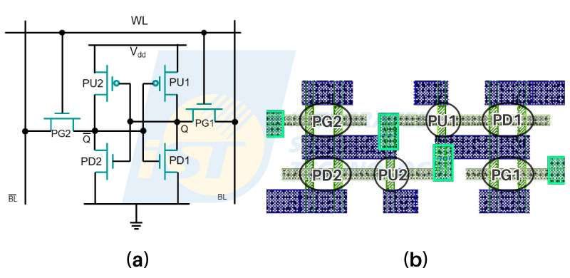
Figure 1: (a) 6T SRAM structure; (b) Corresponding 6T SRAM layout (Source: iST)
For both read and write operations in a 6T-SRAM cell, the Word Line (WL) must be activated. During a write operation, the bit lines (BL and BL) are set to specific voltage levels to force the storage nodes Q and Q within the bit-cell to switch states. When writing a ‘1’, BL is set to the supply voltage for the drain (VDD), and BL is set to 0. Conversely, BL is set to 0, and BL is set to VDD as writing a ‘0’. The write operation uses external voltage sources to change the contents of the bit-cell (Q,Q)from external load.
For reading data from SRAM, the WL is also activated and pulled to VDD. The main difference from the write operation is the state of BL and BL. Before reading, BL and BL must be pre-charged to the same voltage level, typically VDD or (VDD – VT). The read operation balances the external BL and BL (pre-charge), allowing the internal bit-cell(Q, Q)contents to influence the external BL and BL. A sense amplifier is required to amplify the small signal from bit cell to compare the difference between BL and BL to recognize the read-out data as ‘0’ or ‘1’ accurately.
2. Common SRAM Failure Modes
Prior to conducting failure analysis, iST recommends you to confirm the failure mode of each SRAM issue, which will facilitate the process of SRAM analysis. Based on the SRAM operation principles discussed earlier, we can categorize SRAM failure modes into several common types: single bit failure, twin bit failure, quad bit failure, partial bit line failure, bit line failure, word line failure, and block failure (Figure 2).
(1) Single Bit Failure:
Single bit failure can be further grouped as hard single bit failure and soft single bit failure. A hard single bit failure occurs when the bit cannot operate correctly at any operation voltage level, while a soft single bit failure occurs when the bit fails to operate only at specific operation voltage levels.
As initially introduced, PU, PD, or PG are the fundamental components that constitute SRAM. The root cause of a hard single bit failure typically lies in the malfunction of the PU, PD, or PG components, or in the circuitry connecting these components. On the other hand, the failure mechanism of a soft single bit is primarily attributed to micro-leakage or high resistance anomalies in the PU, PD, or PG components, or to the voltage differential between the PU, PD, and PG pairs.
(2) Twin and Quad Bit Failure:
When twin or quad bit failures occur, the analysis focuses on the shared circuitry of the failing bits. Common anomalies as via or metal open/short issue on shared circuit are often observed as the root cause of these categorized failures.
(3) Partial Bit Line Failure:
This failure mode indicates that some bits on a bit line operate normally while others do not. The fault of such failure mode can be revealed on the bit line circuit at the boundary between the normal and abnormal bits.
(4) Bit Line Failure:
Bit line failure is similar to partial bit line failure, but the fault is often located in the bit line control circuits adjacent to the SRAM array rather than within the array itself because the control circuit dominates the bit line operation.
(5) Word Line Failure:
The word line failure is similar to bit line failure, the fault is typically found in the word line control circuits adjacent to the SRAM array.
(6) Block Failure:
The concept for block failure FA is similar to bit line or word line failures, the fault is located on the block control circuits, which is managing the failed block adjacent to the SRAM array.
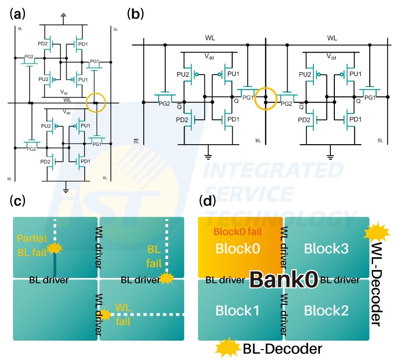
Figure 2: (a) Vertical twin bit failure. (b) Horizontal twin bit failure.
(c) WL/BL failure: abnormality at the WL/BL driver, and partial BL failure: abnormality in the BL metal. (d) Block failure: abnormality at the WL or BL decoder.
(Image source: iST)3. Common SRAM Failure Analysis Methods
Next, iST failure analysis expert team will introduce the failure analysis methods for each of the SRAM failure modes listed above.
(1) Single Bit Failure Analysis:
When encountering such anomalies, the iST failure analysis lab first performs a sample delayer preparation process on the relevant circuit layers (e.g., Metal3) for Focused Ion Beam (FIB) failure bit marking (Figure 3) to ensure precise failure bit localization. We then use Scanning Electron Microscopy (SEM) and Conductive Atomic Force Microscopy (C-AFM) to reveal the defects layer-by-layer from the topmost circuit layer of the SRAM structure. If the metal layers are excluded as fault locations, we can use nano-probe electrical measurements (Nano Prober) to characterize the electrical properties and isolate the faults of the PU, PD, or PG components. Based on the SEM and electrical measurement results, further FIB or Transmission Electron Microscopy (TEM) analyses enables the physical anomaly identification, aiding in corresponded actions for root cause investigation and improvement resolution.
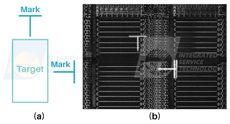
Figure 3: (a) Marking schematic diagram. (b) DB FIB Mark SEM image.
(Image source: iST)(2) Twin and Quad Bit Failure Analysis:
For these failure types, we first perform delayer sample preparation to the relevant circuit layers (e.g., Metal 5) for FIB marking, enabling precise failure bit localization. We then use SEM and C-AFM to search layer by layer from the topmost circuit layer of the SRAM structure. Using SEM and C-AFM, we analyze the shared lines of the failed bits, and then use subsequent FIB or TEM analyses to identify the root cause.
(3) Partial Bit Line Failure Analysis:
Before performing delayering destructive analysis, this failure mode can first be localized using hotspot detection tools, Optical Beam Induced Resistance Change (OBIRCH) and Indium Gallium Arsenide Micro-Optical Microscopy (InGaAs), to identify hotspots for localizing the abnormal area. Following this, the delayering, FIB marking, and analysis methods mentioned above are used for the root cause investigation.
(4) Bit Line Failure/Word Line Failure/Block Failure Analysis:
These failure modes are related to the peripheral circuits of the SRAM. Such anomalies can first be localized using hotspot detection tools, OBIRCH and InGaAs, to identify fault location, followed by de-layering based on the hot spot locations, and then using SEM, C-AFM and Nano Prober analysis methods to confirm the defects. Subsequent FIB or TEM analyses can then be performed to identify the root cause.
4. SRAM Failure Analysis Case Studies
(1) Hard Single Bit Failure Case:
In this single bit failure case, there is a short circuit between the structure connecting PD1 and PU1 (Butted contact) and the structure connecting PD2 and PU2 (another butted contact) (Figure 4). Since these two connected structures have the same electrical properties, abnormalities could not be detected using SEM VC and C-AFM (Figure 5(a)(b)). In this case, we utilized Nano Prober to probe the two structures, revealing the abnormal short circuit between these two circuits that should not be connected originally (Figure 6).
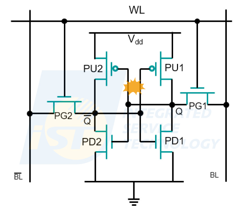
Figure 4: Structure diagram corresponding to VC abnormality location
(Image source: iST)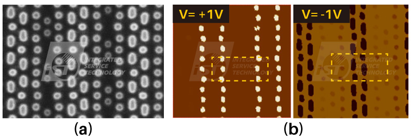
Figure 5: (a) SEM VC image of contact layer in single bit failure
(b) C-AFM image of single bit failure
(Image source: iST)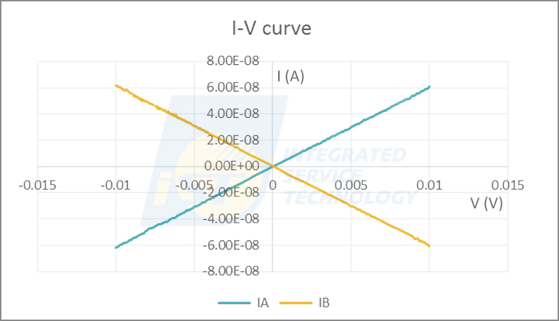
Figure 6: Measurement with Nano Prober confirming short circuit in Butted contact
(Image source: iST)(2) Soft Single Bit Failure Case:
In this case, the two inverters within the SRAM cell have inconsistent switching voltages, causing a soft single bit failure. In this situation, we cannot detect abnormalities using SEM VC inspection. Therefore, we implemented Nano Prober to measure the electrical properties of the six transistor components within the SRAM individually. The results showed that the failed bit’s PD1 had a threshold voltage significantly higher (over 100mV) with another normal PD(PD2). After the circuit designer fed this measurement data back into the circuit simulation, it was confirmed that the threshold voltage difference is significantly caused such soft single bit failure (Figure 7).
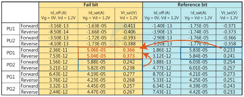
Figure 7: Measurement with Nano Prober confirming PD1’s threshold voltage is over 100mV higher than that of a normal transistor
(Image source: iST)(3) Horizontal Twin Bit Failure Case:
This type of anomaly occurs between two adjacent bits sharing the same word line, typically happening in the shared circuit structure of the two bits (Figure 8(a)). After de-layering to the highest shared layer based on the circuit analysis, abnormalities in the shared connection to the bit line can be observed using SEM VC (Figure 8(b)). Further Cross section FIB or TEM analysis of the abnormal location reveals a process abnormality causing an open circuit beneath the observed VC abnormality.
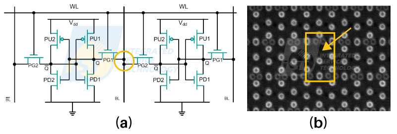
Figure 8: (a) Circuit diagram of horizontal twin bit failure abnormal location
(b) Abnormal SEM VC image
(Image source: iST)(4) Vertical Twin Bit Failure Case:
This type of anomaly occurs between two adjacent bits sharing the same word line. Similar to analysis concept in the horizontal twin bit failure investigation, these anomalies typically occur in the shared word line circuit structure of the two bits (Figure 9(a)). After de-layering to the highest shared layer based on circuit analysis, abnormalities in the shared connection to the word line can be observed using SEM VC (Figure 9(b)). Further Cross section FIB or TEM analysis of the abnormal location reveals a process abnormality causing an open circuit beneath the VC abnormality.
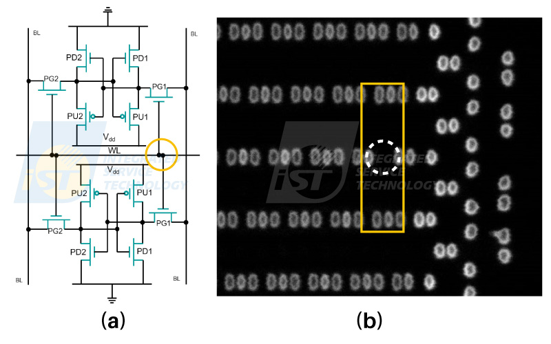
Figure 9: (a) Circuit diagram of vertical twin bit failure abnormal location
(b) SEM VC image of Via0 layer in WL failure case
(Image source: iST)
As analyzing an SRAM product failure and consistently failing to have zero hit rate on locating the defects, it is necessary to re-confirm whether there is a mismatch between the electrical address and the physical address of the bit. At this point, iST failure analysis experts recommend to conduct a scramble to verify the translation between electrical and physical bit locations.
Scramble check is mainly used for verification in the early stages of new product development. After discussing with the circuit designer, specific word lines or bit lines, or even specific bits are selected first. FIB IC circuit edit techniques are implemented to cut these lines proposed by the designer to create artificial failure locations. The product testing program is then used to confirm the failure locations. With the electrical testing results, we can therefore identify the correlation between electrical address and physical address. After the scramble check verification, the possibility of not finding the correct analysis location in SRAM product failure analysis can be eliminated.
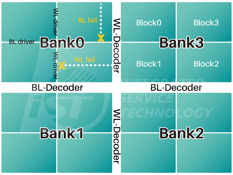
Figure 10: Schematic diagram of WL & BL cuts
(Image source: iST)
This article is shared with those who have long supported iST. If you need a SRAM failure analysis flow chart, please contact us, and we will provide a meticulously crafted chart for your reference. Please contact +886-3-579-9909 ext. 6775 Mr. Shi (CY) │Email: web_ISE@istgroup.com;marketing_tw@istgroup.com。