Issued Date:2023/2/7 CIS Chip defect
Issued By:iST
Do you ever feel helpless over the defects on CIS chips with its thinner die and 3D stacking structure?

CMOS Image Sensor (CIS) technology development is originated from the human demand for higher resolutions and pixels. Thanks to the evolution of Moore’s Law, the continuous semiconductors process miniaturization significantly improves signal processing capability and enables the migration of CIS resolution from below-zero megapixels in earlier times toward 100+ megapixels. However, the failure analysis for CIS chip defect become more complicated during R&D or mass production stage for such advanced CIS products.CIS Chip defect
So, how to dig out these CIS chip defects? Before starting this session of the iST Classroom, let’s introduce the types of CIS chips.
CIS Chip defect
CIS Chip defect
1. Understanding 3 Major Types of CIS Chip Architecture
Currently, there are three major types of CIS chip, including the (1) Front Side illumination (FSI), (2) Back Side illumination (BSI) and (3) Stacked CIS.
(1) FSI CIS
In order to manufacturing CIS chips by typical semiconductor process for mass production, FSI CIS (first type), the light sensing path receives light via the front side of the CIS chip, is designed and developed. However, the light interference from the metal layer above the image sensor is the fatal problem of FSI CIS performance, reducing the quantum efficiency and attenuating light sensibility of sensors.
(2) BSI CIS
Hence, BSI CIS was introduced to improve the light sensibility of CIS chips thereafter. By receiving light from the thinned backside of chips, down to a few micrometers, BSI CIS has significantly light sensing capability enhancement.
As for the BSI CIS process, the main difference lies in the additional wafer bonding and silicon substrate thinning down process, while both BSI CIS and FSI CIS adopt similar front-end processes. After the CIS process to form sensing diodes and backend metal routing, the front side of CIS wafer is bonded to a carrier wafer, which is the supportive structure to sustain the chip mechanical robustness after the thinning process of the backside CIS wafer. Then, backside grinding process is implemented on the bonded CIS wafer to thin the wafer to a few micrometers in order to enhancing light receiving efficiency. This is how the BSI CIS is made.
(3) Stacked CIS
With widely and boosting demands of consumer electronics applications, people are urged for higher image processing capability on their taking photos and videos with friendly product price. With the implementation of wafer stacking process, the CIS wafers can be processed by bonding CIS sensor wafers with mature process, ASIC wafers with advanced process for providing powerful computing capability, and even DRAM wafers together for a high-performance and cost-effective stacked CIS (Figure 1).
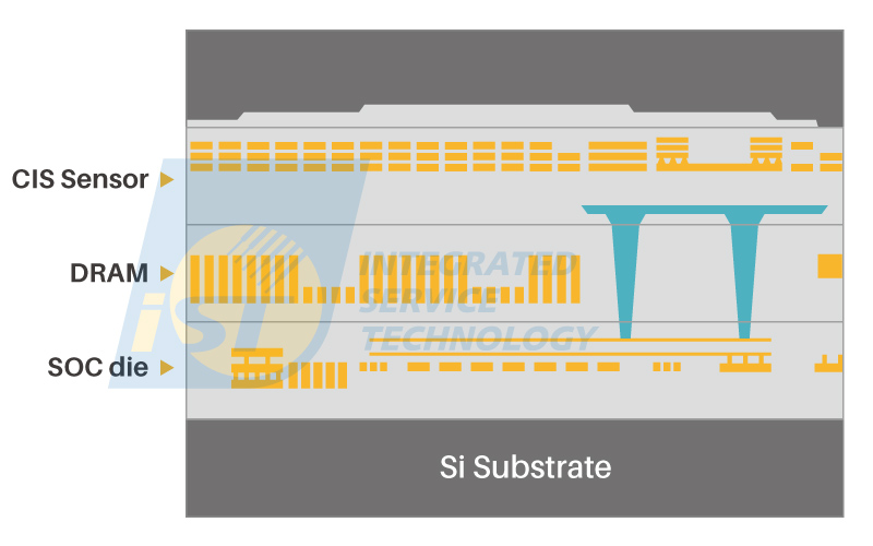
Figure 1: Illustration of the stacked CIS chip.
2. How to dig out defects on stacked CIS chips
After the introduction of those three major types of CIS scheme, let us move to the focus of today’s iST Classroom: How to find defects on stacked CIS chips? Due to the structural complexity of stacked CIS chips, it is necessary to perform fault isolation to narrow down the fault location by circuit edit or hotspot inspection process before the destructive analysis. Then, the destructive failure analysis process is implemented on the suspected failure area of the analyzed CIS sample to dig out the physical failure evidence in order to taking further corrective and preventive action for the failures.
Subsequently, we will show you how the iST Failure Analysis Lab perform failure analysis on stacked CIS chips through the implementation of the following methods to dig out the defects efficiently. These methods are: (1) fault localization (hotspot detection), (2) layer-by-layer analysis on the target area, (3) electrical characteristics measurement (C-AFM & nano-prober) and (4) scanning acoustic tomography (SAT).
(1) To dig out the defect of hot spots with Thermal EMMI
When electrical failures, such as high resistance, short, leakage, or function failures, are found on a CIS chip, OBIRCH、Thermal EMMI(Figure 2), or InGaAs are well-selected and utilized for finding out the fault location by hotspot inspection based on different types of electrical failure modes, with applying DC power directly or testing pattern powered by test board, and facilitate the subsequent success Physical Failure Analysis (PFA).
● Timing for use of different types of equipment
Detection tool OBIRCH Thermal EMMI InGaAs Detection level Device / Metal Metal / Package
Level/ PCBDevice / Metal Failure mode Leakage, Short,
High-RLeakage, Short, High-R Leakage, Short, Open 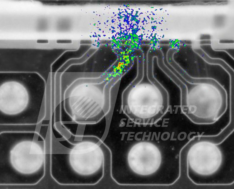
Figure 2: Thermal EMMI is utilized for electrical failure analysis (Short failure in this example)
(2) Layer-by-layer analysis on targeted dies
After fault isolation process, defect can be isolated on the light sensor, ASIC or DRAM chip, the Si substrate on non-interested side of the analyzed CIS chip can be removed first and then perform layer-by-layer process to reveal the physical of failure.
iST Failure Analysis Lab has successfully developed an unique solution to remove the unwanted parts of the CIS chip and expose the top metal layer (Figure 3) of the target area. With layer-by-layer removal and inspection, the burnout anomaly was found on Metal 1 (Figure 4) in this example.
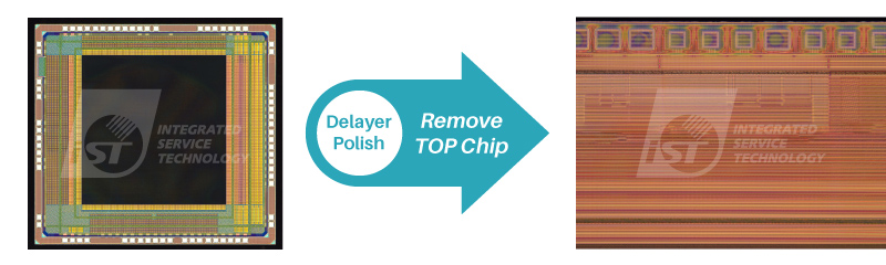
Figure 3 : With the special method developed by the iST Lab, the unwanted parts of a die on the CIS under test are removed.
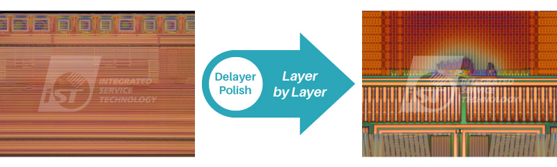
Figure 4: The burnout anomaly was found after proceeding with the layer-by-layer removal on the target chip based on the range of hot spot analysis.
(3) Electrical Characteristics Measurement (C-AFM and Nano-prober)
Besides of verifying electrical behavior through Voltage Contrast (VC) and inspecting the metal routing profile around the interested zone with SEM during the layer-by-layer removal, C-AFM analysis on the interested area can also be implemented to measure the electrical performance by obtaining the Current map (Figure 5) of that area in order to verifying if any leakage or open electrical faults can be observed.
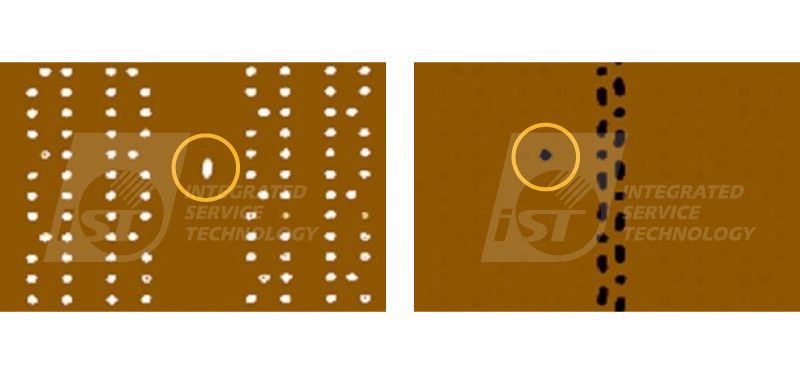
Figure 5: Results of C-AFM defect analysis.
Figure 5 (left): An electrical anomaly was found in the Current map, scanned by C-AFM, when applying positive voltage (+1V) on the analyzed sample (circled area).
Figure 5 (right): An electrical anomaly was found in the Current map, scanned by C-AFM, when applying negative voltage (-1V) on the analyzed sample (circled area).If further electrical measurement and/or fault isolation are required on suspected defective paths after C-AFM analysis, Nano-Prober can be utilized for more accurate electrical fault isolation analysis, including Electron Beam Induced Current (EBIC), Electron Beam Absorbed Current (EBAC), and Electron Beam Induced Resistance Change (EBIRCH). (Further reading: Methods of precise positioning for defect detection based on nanoscale electrical characteristics measurement)
The Nano-Prober can also be performed electrical measurement on chips, such as obtaining the fundamental device characteristics (Vt, IdVg, IdVd, etc.) (Figure 6).
With the precise defect localization with the above methods, Dual-beam FIB or TEM can also be used to reveal the physical defects for further failure root cause investigation (Figure 7).
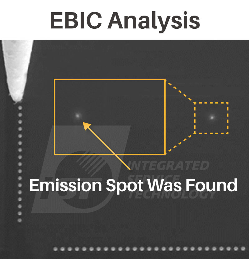
Figure 6: Results of EBIC analysis
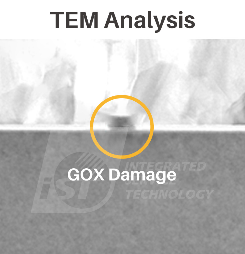
Figure 7: Results of TEM analysis
(4) Scanning Acoustic Tomography (SAT): Application on wafer bonding process of BSI/Stacked CIS chips
SAT is an analyzed tool to analyze the material interface quality or behavior by means of different material characteristics in reflection speed and energy from ultrasound signals transmission. When contacting the bonding interface of different materials, part of the ultrasound signals will reflect back to the detector and part of the ultrasound signals will penetrate the bonding interface. When contacting air (voids), 100% of signals will be reflected to the detector to form the image with arrowed areas (Figure 8).
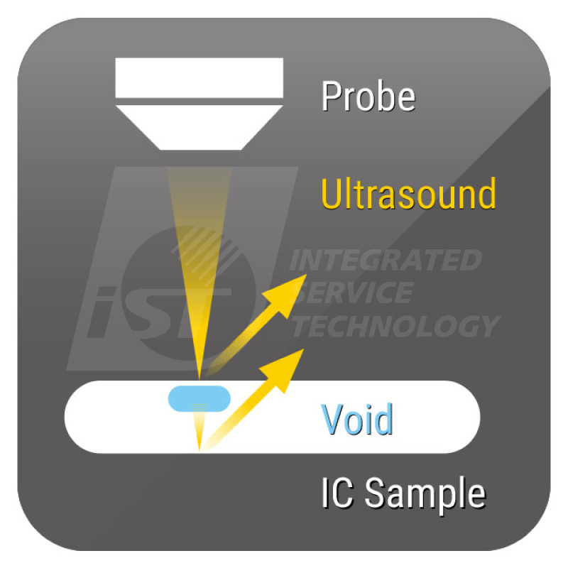
Figure 8: Principles of SAT.
在Wafer bonding is a very critical process in BSI and Stacked CIS. In the wafer bonding process of BSI CIS and Stacked CIS, SAT is a powerful tool to detect if any bonding voids in-and-between the bonded wafers (Figure 9).
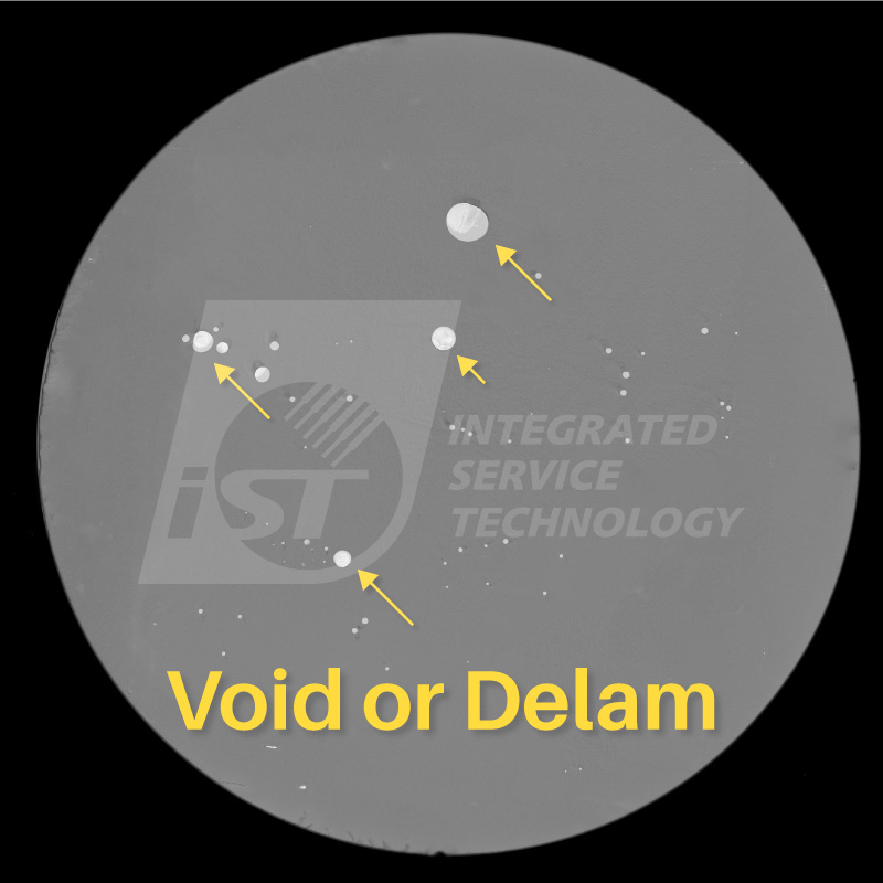
Figure 9: Bonding voids were found in bonded wafer with SAT implementation.
With the widely adoption of the stacking technology and boosting CIS demands from consumer electronics, automotive electronics, and security control systems, stacked CIS will become the mainstreamed CIS products in the near future. In addition to the well-developed failure analysis methods for FSI CIS and BSI CIS, iST Failure Analysis Lab can also offer wafer bonding stability analysis or Stacked CIS failure analysis service with its developed unique analysis methods and one-stop integrated service to help you have effective analysis on your analyzed chips, in order to accelerating your product development and improving product quality.
For more information about reverse engineering to prevent patent disputes, please feel free to contact Mr. Li ext. 6612 by email to
IST_FA_IAD@istgroup.com or marketing_tw@istgroup.com
Other services you may be interested in
CIS Chip defect