Issued Date:2020/12/15wafer ultra thinning
Issued By: iST
Power semiconductor is the hot topic now and is a future trend which, in turn, forced us to face and deal with the process risks that come with wafer thinning.
Wafer Ultra Thinning
Wafer thinning has been the most direct and effective process improvement in cutting power consumption and input impedance of power semiconductors which not only reduce packaging dimension but also extends the service life of wafers by lowering RDS (on) and heat accumulation.
However, the MOSFET foundries are facing a challenge of balancing thinness and strength of wafers to minimize the risks of soaring rate of broken wafers.
wafer ultra thinning
iST has developed the thinning technology for wafers 2mil, 1.5mil, and even 10um thick. The silicon chips shown in Figure 1 are so thin that red light can penetrate the wafers when white light source on their backside.
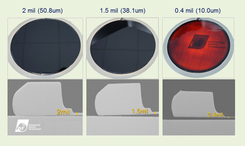
Figure 1: From Scanning Electron Microscope (SEM) results, the X-SEM of 50um, 38um, and 10um thinned wafer
Let’s explore ways to improve the strength of thinned wafers.
I. In Terms of Wafer Grinding
The thickness of 8″ primary wafer is 725 um (28.5 mil) can be reduced to 50 um (2 mil), 38 um (1.5 mil) or even 10 um (0.4 mil). The surface damage layer by TEM analysis shows that the depth of the damage layer goes along with grinding level (Figure 2) which result in mechanic stress accumulation, poorer die strength and a more demanding packaging and testing process. The iST exclusively optimized process to take up this challenge and rise production yield (Figure 2).
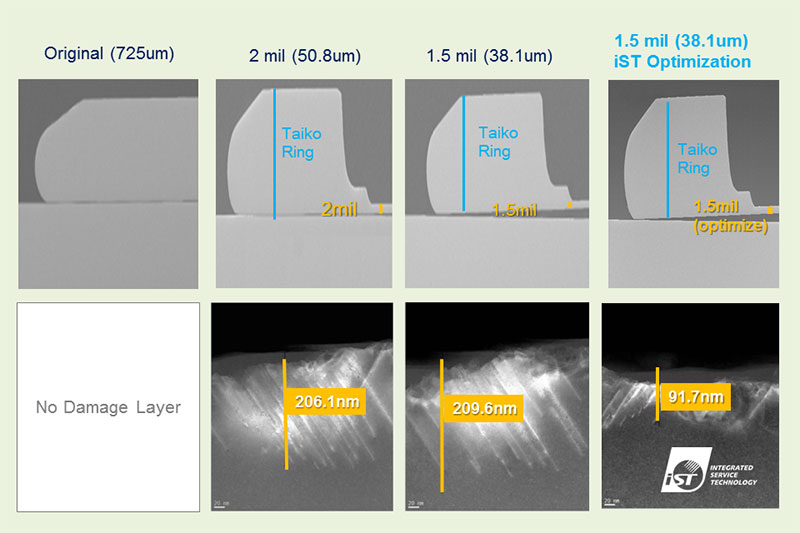

Figure 2: TEM maps of damage layers in thickness of 2mil, 1.5mil and 1.5mil after optimization by using control wafers
II. In Terms of Wafer Etching
The purpose of the wafer etching process is not only to get wafer thinned but also strengthened by reducing stress accumulation at the damage layer through mechanical grinding as shown in Figure 3.
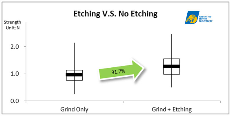
Figure 3: Increase wafer strength through etching process to reduce stress accumulation (Data normalized).
Through professional die strength test employed by iST, the optimized etching process can enhance the wafer strength to meet customer’s specification requirement as shown in Figure 4.
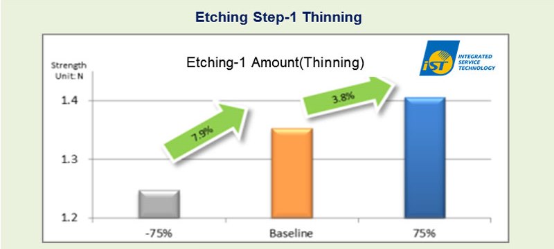
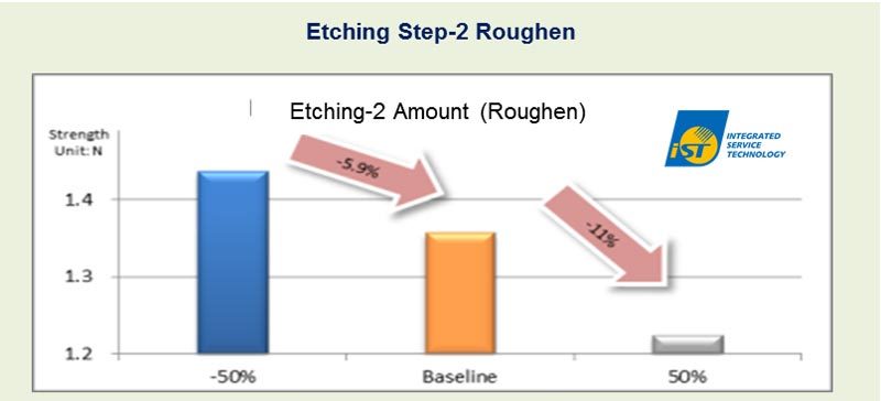
Figure 4: Optimize the etching conditions to obtain higher strength and lower stress (HsLs) to facilitate following processing (Data normalized).
iST can provide you with customized solutions to enhance your wafer for Power MOSFET/IGBT and other components. Should you have any inquiries, just ring Mr. Yu(Stan) at +886-3-579-9909 EXT 5888 or email us at web_sp@istgroup.com