Issued Date: 2019/6/11
Issued By: iST
How to debug packages composed of multiple chips and components, including SiP, MCM, MCP, and QFP?
How to determine the correct test result without interference from other device components?
While more functions are cramping into single high-tech devices with increasingly shrinking dimensions, system integration among device components are focusing on electronic communication and information products, which is pushing the industry toward System in Package (SIP), Multi-chip Module (MCM), Multi-chip Package (MCP), and Quad Flat Package (QFP).
Nevertheless, a good die is the MUST requirement for these package types. As it is packaged in the single IC of multiple components or ICs, even one defective die of them may hamper the operation of all the components and ICs. Thus, it’s very important to analyze and test individual ICs in any MCM.
To identify failure of the single component which results in defective IC is a tall order. Internal wiring and board circuit connections among SiP, MCM, MCP, and QFP tends to suffer in electric tests by interference of other chips or device components which, in turn, makes test results hard or even impossible clear.
iST is sharing the means to deal with this issue in iST Tech Classroom this month. With years of experiences in semiconductor verification and analysis, iST has come up with IC Repackaging technology to repackage target dies out of SiP, MCM, MCP, and QFP package into other types of packaging for electric tests.
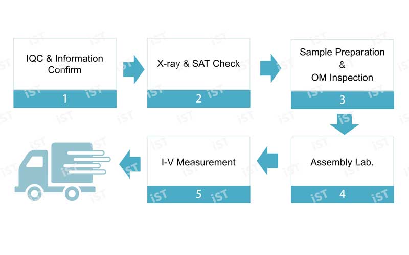
IC Repackaging in 5 steps
The iST lab executes IC Repackaging in 5 steps. Step 1) Subject sample-for-testing (SFT) received to Incoming Quality Control (IQC), counting and validating them against information provided by customer (including appearance inspection of SFT and quantity, position, and thickness of dies inside package). Step 2) Check if any packaging abnormal with X-ray or SAT (Scanning Acoustic Tomography) inspection and locating dies to be removed. Step 3) Remove dies with acid etching and grinding, then inspect whether cracks, burnouts, chipping and other defects or not with digital 3D OM. Step 4) Repackage dies and wire bonding into specific packages required by the customer. The last step is for iST to pre-check IV electric characteristics measurement over the ICs repackaged or directly returned to the customer for functional/electrical characteristics measurement and verification.
Figure 1: IC Repackage in 5 steps
Typical IC Repackage Case
Employing its IC Repackaging technique, iST removes one die out of a QFP, as shown in figure 2 below, and repackages it into wBGA packaging type. This helps the customer to execute overall review and electric tests over standalone IC as well as enables it to undergo tests at the customer’s factory.
Figure 2: Remove and repackage single die from QFP into wBGA packaging for later tests
Should you have any inquires for sample repackages, please call Ms. Chang (Susen) at +886-3-579-9909 Ext. 6795 or send an email to web_ise@istgroup.com


