Issued Date: 2017/3/29
Issued By: iST
Sadly, your IC device failed due to high resistance and current leak!
Your customers are pushing for a solution (report) while you are trying to pinpoint where it failed!
Did it fail somewhere on the XYZ axis? Where do you start finding defects in 3D-IC?
The 3D chip stacking technology for improved electronic product performance comes with its own problems, it’s much harder to pinpoint defects encountered. For devices packaged in conventional mechanism it’s easy to identify defects by just scanning the 2D plane of the X- and Y-axis. This is not the case with 3D devices as the Z-axis position is as important as its two counterparts, let alone the difficulties in pinpointing failures brought by vertically stacked layers.
Don’t worry, these three simple steps by iST may assist you catching 3D device defects with ease. See how iST is applying them in finding the causes of current leaks found in 3D devices.
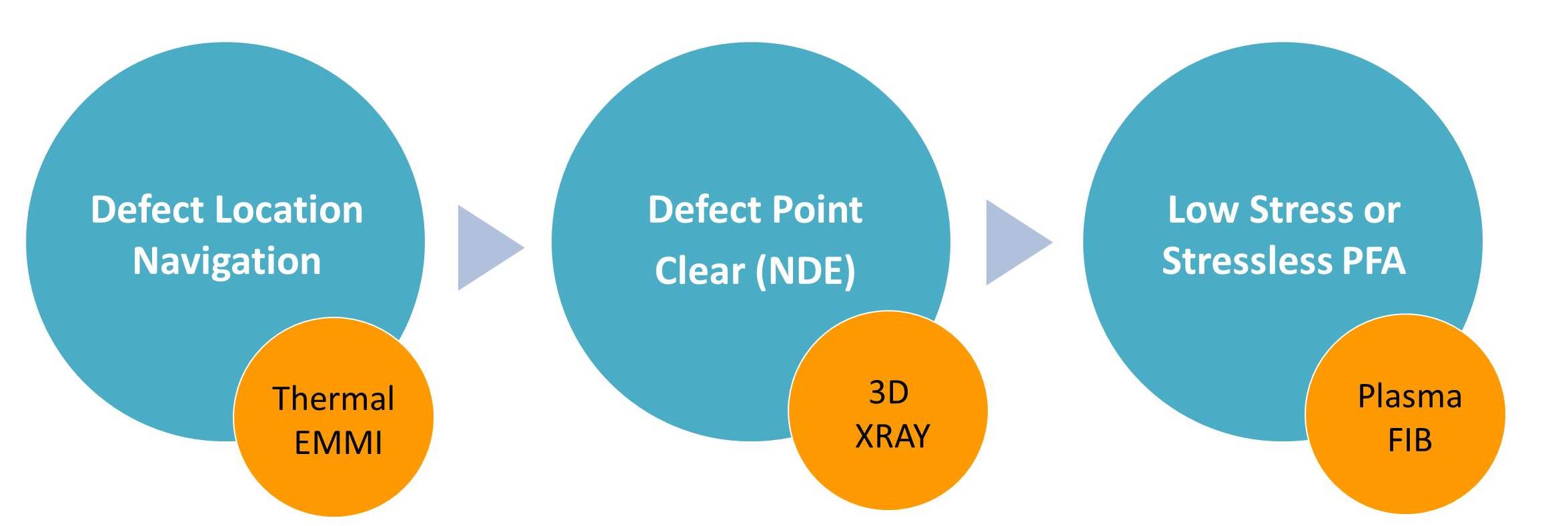
Step 1: Localization
Detect failure depth (Z-axis direction) of 3D packages by phase differences of thermal radiation at the failure point without damaging powered 3D devices to quickly position the failure point (getting its XYZ coordinates) and, in turn, concluding that the defect falls at the solder ball (see figure below).
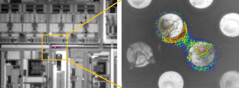
Image by thermal EMMI
Step 2: Imaging
Without invading the device, the 3D X-ray system presents an image at the failure position in a 3D and cross section view. The 3D image at the lower left suggests the defect point is located at the solder ball while the 3D cross sectional analysis pinpoints its position at solder balls close to the UBM layer.
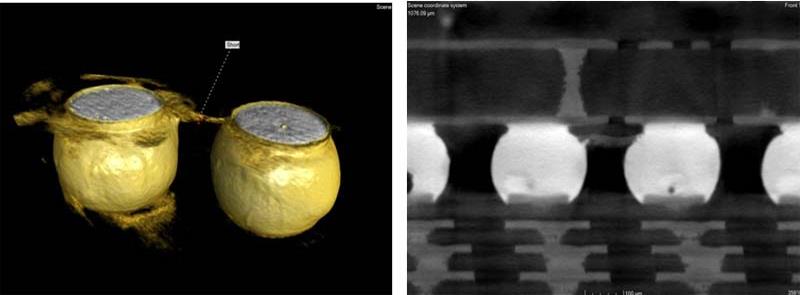
3D diagram
3D cross sectional diagram
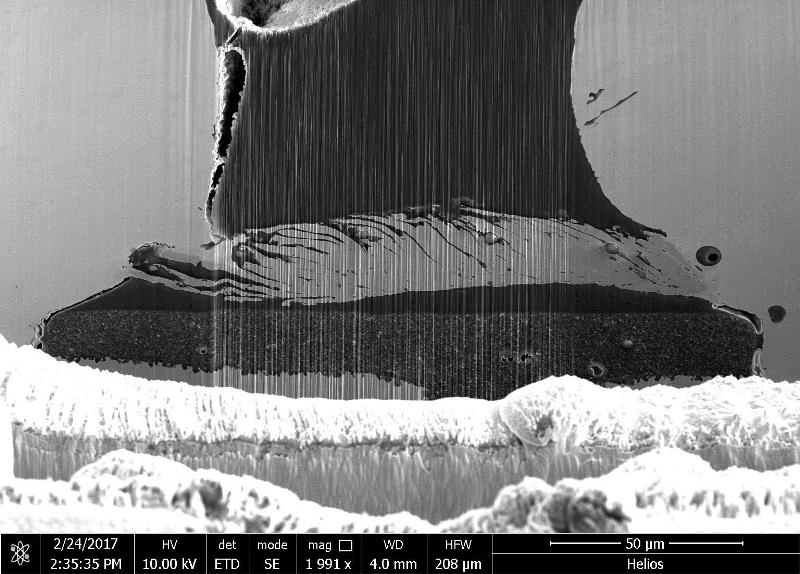
Step 3: Cutting
3D devices suffer stronger stress by aligning packaging material (BOM). It requires low-press tools as adjacent layers tend to break when external forces are applied to them. As stress by conventional manual grinding may lead to severe damage, a low-stress plasma-FIB is used to cut out failed section for cause identification. The results: there is RDL bridging in between solder balls of the component (see diagram below).
We are more than glad to share our inspection and test experiences with you. In case of any needs to identify causes to defects in 3D devices or further information on relevant knowledge, please call Mr. Chen (Teron) at +886-3-579-9909 Ext. 6767 or email her at web_ise@istgroup.com.