Issued Date:2025/2/18Circuit Edit
Issued By:iST
Did cutting the wrong circuit give you a headache? This edition of iST classroom takes you through the ultimate guide to FIB (Focused Ion Beam) circuit edit! Empowering engineers to escape the debugging hell and efficiently complete design validation.
Circuit Edit
In IC design, even if simulation results look flawless, unexpected circuit anomalies can still arise once implemented on the chip. This isn’t just about the cost of re-taping; it can also delay project timelines and put pressure from clients. Worse, when circuits fail, engineers often struggle to locate the defect or determine where to connect or cut, turning debugging into a daunting task.
This is where Focused Ion Beam (FIB) circuit edit comes into play. It allows for quick and flexible circuit repairs, completing design validation with minimal cost and time, and breaking free from endless debugging cycles.
As the first private lab in Taiwan to offer FIB circuit edit services, iST’s solutions save 3 to 6 weeks of development time in IC design and reduce mask re-taping costs by millions, accelerating time-to-market for products. iST’s FIB lab also operates 24/7, supporting clients in debugging and identifying root causes efficiently.
In a previous edition of the iST classroom, we introduced how to perform FIB circuit edit on advanced process ICs, the advantages of back-side modifications, and examples of complex cases (Read more: How to Do Backside FIB Circuit Editing for Advanced Process IC? And What is the Challenge in Editing the FIB Circuit on a 5nm Chip?).
In this edition of the iST classroom, we are sharing 30 years of iST’s FIB circuit edit experience to help you fully understand this essential technology, speeding up debugging and enhancing design efficiency!
Circuit Edit
Circuit Edit
1. Basic Principles of FIB
Focused Ion Beam (FIB) Electron Microscope utilizes a gallium (Ga+) ion source, which is extracted into an ion beam through an electric field. The system collects secondary ions and electrons generated by high-speed collisions with the sample surface to create images. During ion bombardment, different gases are injected to selectively accelerate or decelerate etching of various materials on the chip, as well as to deposit conductive or dielectric insulating materials, achieving circuit edit. Combined with a CAD navigation system, this technology accurately locates targets and enhances the precision of circuit edit.
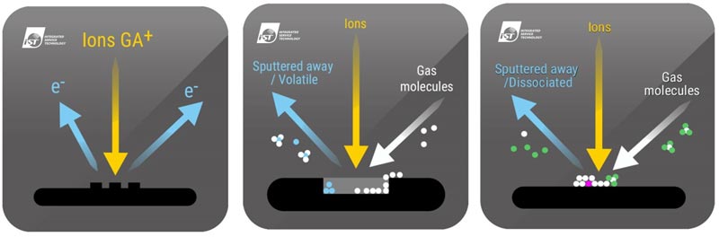
Imaging mechanism
Etching mechanism
Deposition mechanism
2. Why Perform FIB Circuit edit?
Just like a surgeon uses precise microsurgery to address a patient’s physical defects and improve their health, iST’s FIB Lab applies professional and meticulous FIB circuit edit to pinpoint issues before chip tape-out. This process significantly reduces the high costs of re-taping, accelerates prototype validation, and shortens time-to-market. The FIB circuit edit also supports clients under tight development schedules by enabling small-scale revisions for production, allowing samples to be sent to end customers for validation. This approach helps clients gain a competitive edge and secure orders.
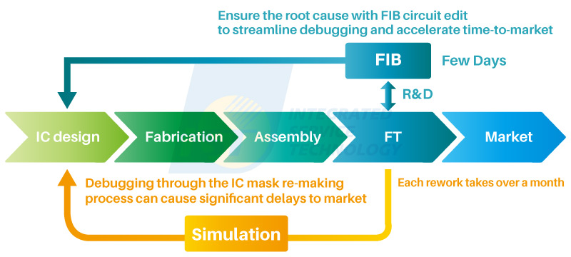
Figure 1: FIB Circuit Edit Reduces IC Reproduction Costs and Prototype Validation Time
(Source: iST)FIB leverages etching to remove insulating and metal layers, followed by metal deposition to reconnect circuits to other pathways. This process can be performed with precision according to customer requirements and allows for testing to identify and confirm issues within the circuit.
Using a cross-section view, we can clearly observe how focused ion beam technique precisely removes surface materials to expose the target metal layers. The process then deposits metal to fill the contact and bridges the connections on the chip surface, enabling circuit reconnection. Subsequent testing verifies whether the circuit’s functionality aligns with simulation results.
Additionally, depending on specific requirements, more complex circuit reconstructions can be executed, further expanding the range of solutions. Clients can use testing results to identify circuit defects and address diverse debugging needs effectively.
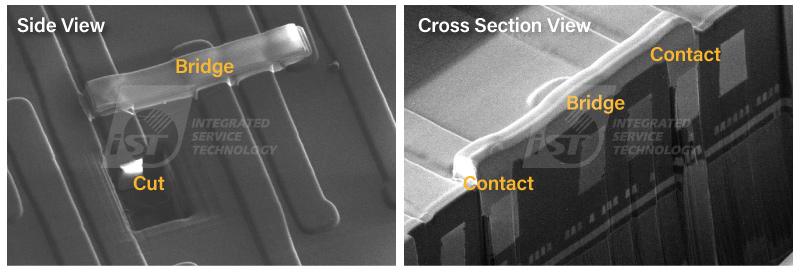
Figure 2: Cross-Section of the Circuit After FIB Circuit Edit
(Source: iST)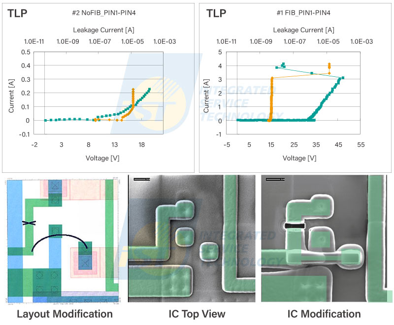
Figure 3: FIB Circuit Edit Connecting Design Defect to ESD Protection Circuit, Increasing Current Tolerance from 0.2A to 4A (TLP Test)
(Source: iST)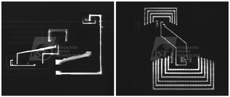
Figure 4: Focused and Multi-Target Circuit Edits Performed Based on Customer Requirements
(Source: iST)3. Wide Applications of iST FIB Circuit Edit
iST’s FIB circuit editing has advanced to support 3nm node and offers both front-side and back-side circuit edit services. With a diverse range of equipment and ample capacity (Table 1), iST can meet high-volume demands while providing flexible and customized solutions. This ensures high yields and fast turnaround times.
In addition, iST’s experienced technical team is proficient in operating various equipment and uniquely offers circuit edits on 8-inch wafers without breaking them—an exclusive service in the Taiwanese market. This capability sets iST apart, providing unmatched options for customers in the region.
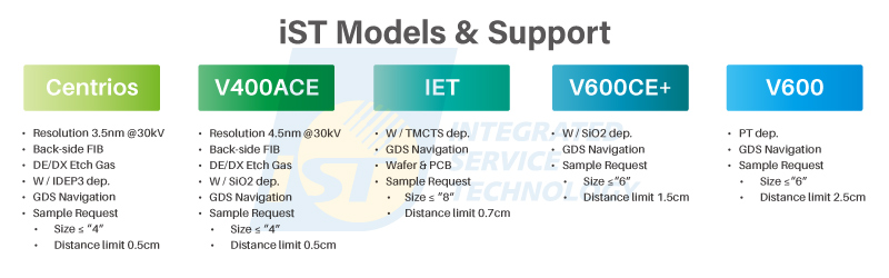
Table 1: Equipment and Sample Limitations of iST’s FIB Circuit Editing Laboratory
(Source: iST)As shown in Figure 5, FIB circuit edit can be followed by different kinds of tests, such as electrical measurements, fault isolation, material analysis, and quick package assembly. Below, we will detail the various broad applications of FIB technology.
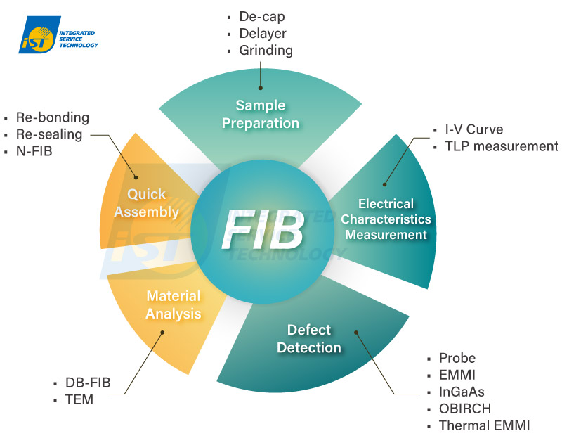
Figure 5: Post-FIB Circuit Edit Experiments, Including Failure Analysis and Material Analysis, Enabling Rapid Defect Localization and Issue Resolution
(Source: iST)(1) Adjusting Resistance by Depositing Metal Materials Using FIB
FIB circuit edit can connect circuits by depositing metal materials. Moreover, it can be further applied to adjust resistance values based on customer requirements. By depositing metals with different resistivity, such as tungsten or platinum, between two circuit connections, the length of the metal connection can be controlled to achieve precise resistance adjustments. This method allows for the simulation of how varying resistance values affect circuit performance. Additionally, it supports subsequent experiments, such as waveform analysis (I-V curve) and ESD-related failure analysis measurements.
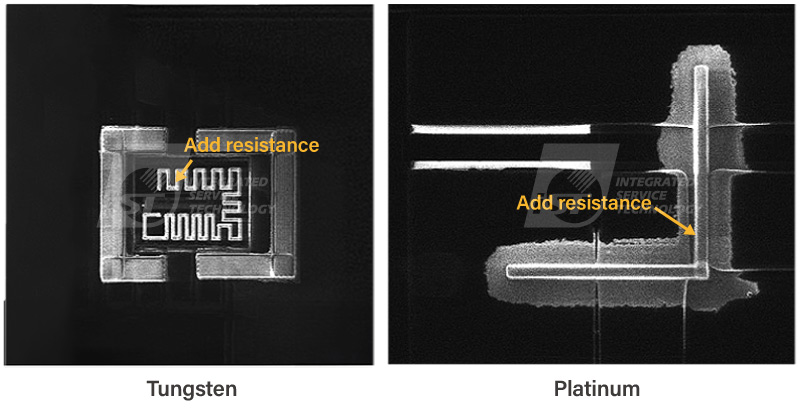
Figure 6: Adjusting the Length of Tungsten or Platinum Metal Deposits Between Two Circuit Connections to Add Resistance
(Source: iST)(2) iST’s Unique Customized FIB PAD Design Facilitates Smooth Electrical Testing of IC
iST’s FIB PAD features a cross-shaped design, enabling probes to stabilize securely at any inner angle, preventing probe holder slippage. This design also allows multi-directional adjustments, making it easy to reposition the probe holder in case of poor contact. This ensures optimal connectivity and reusability, enhancing operational stability and extending the PAD’s lifespan.
iST can further customize more advanced and complex FIB PADs to meet customer requirements. Using precision probing techniques, signals can be accurately captured to test whether circuits in the target area comply with design specifications. This facilitates real-time defect identification and localization. Subsequent steps may include circuit edit to resolve issues or hot spot analysis to pinpoint anomalies. For defective areas, cross-section FIB or TEM analysis can be conducted to verify process-related defects.
Additionally, iST’s FIB lab is equipped with dielectric insulating materials, enabling safe FIB operations even on wafer-level semi-finished products or delayered chips. The exposed metal layers are isolated with insulating materials, ensuring safe and precise FIB processing.
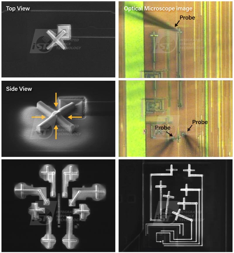
Figure 7: iST Can Customize Multi-Point Probe PADs in Specific Areas Based on Customer Requirements
(Source: iST)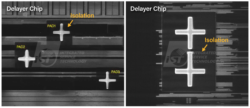
Figure 8: Insulating Materials Cover Exposed Metal Layers During Probe PAD Creation on Delayered Samples to Prevent Short Circuits
(Source: iST)(3) Extended Applications of FIB PAD: New FIB Circuit Repair (N-FIB)
- Low Impedance Solution
Taking a 1,000 μm connection distance as an example, traditional FIB deposition techniques yield an impedance of 6 kΩ for Pt material and 2 kΩ for W material. In contrast, N-FIB technology achieves an impressively low impedance of just 10 Ω, significantly enhancing performance. - Signal Extraction
Replacing traditional probe testing, N-FIB offers greater flexibility and repeatability, making it ideal for more frequent and complex testing demands and environments. - Adding Capacitors or Resistors
N-FIB enables the connection of capacitors or resistors using SMD 0201 packaging (dimensions 300×600 μm), meeting more precise circuit testing requirements.
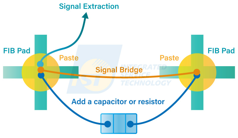
Figure 9: Creating Signal Extraction Points Followed by Signal Bridging, Component Addition, or Signal Routing
(Source: iST)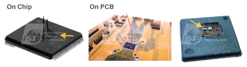
Figure 10: Signal Routing and Component Placement Diagram
(Source: iST)(4) Application of FIB Delayer in Failure Analysis and Nano Probe Testing
When measuring advanced process chips or high-speed signal functionalities, using FIB PADs for testing might introduce additional impedance or capacitance, leading to signal distortion. To address this issue, iST’s Failure Analysis Lab employs Nano Prober equipment for electrical measurements, minimizing signal loss.
Before conducting such measurements, the chip must undergo delayer. Traditional delayer techniques require comprehensive layer-by-layer grinding to the target metal layer, which is time-consuming and increases the risk of over-grinding, especially for advanced process chips.
In contrast, FIB can precisely target localized areas for delayer, significantly reducing the risk of failure. The etching capabilities of FIB make it an ideal solution for achieving efficient and accurate preparation for Nano Probe testing.
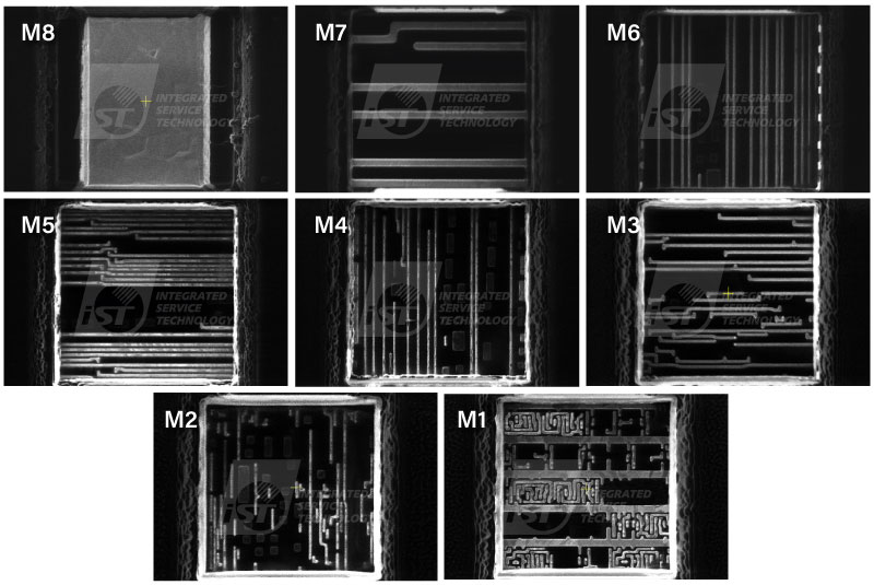
Figure 11: Targeting Localized Areas for Delayer, Precisely Reaching the Desired Metal Layer and Reducing Over-Grinding Compared to Traditional Methods
(Source: iST)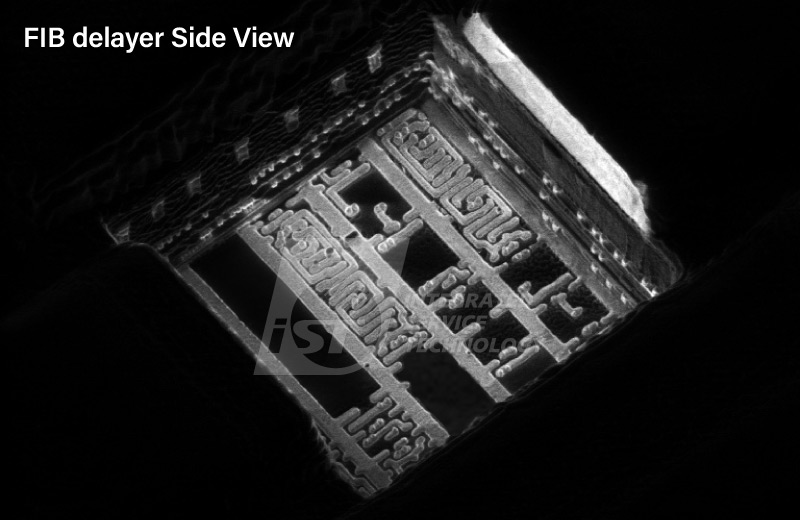
Figure 12: Side View of iST’s FIB Delayer Capability
(Source: iST)(5) FIB Backside Circuit Editing
Backside circuit editing is a well-developed and highly stable technology with a comprehensive workflow, including decapsulation, grinding, and re-encapsulation, each supported by tailored solutions. Notably, localized grinding of the target area enables FIB circuit edits in CoWoS (Chip-on-Wafer-on-Substrate) packages.
When performing backside circuit edits, the target is typically within the M1 to M3 metal layers, which are the layers with critical pitch in the chip. This requires exceptional technical expertise and high-quality imaging from lab personnel. As demonstrated in the example, iST utilizes high-resolution images with a minimum beam current of 1.2 pA, aiding circuit identification and enhancing success rates.
As device size in advanced process node continues to shrink and end-product demands grow, Flip Chip packaging is being increasingly adopted. CoWoS packaging, a form of Flip Chip 2.5D packaging, is a prime example. From a FIB backside editing perspective, Flip Chip packaging offers the advantage of a low aspect ratio and allows modification at the source of the circuit, simplifying the editing process.
However, with process nodes advancing to 7nm, 5nm, 3nm, and even future 2nm, circuit design diversity and complexity are increasing exponentially. While iST has demonstrated successful edits on 3nm nodes, these advanced processes present significant challenges, demanding greater technical and equipment capabilities.
One major future challenge for FIB circuit editing lies in addressing Backside Power Delivery Network (BSPDN), a cutting-edge technology in the market, as it becomes more prevalent in next-generation chips.
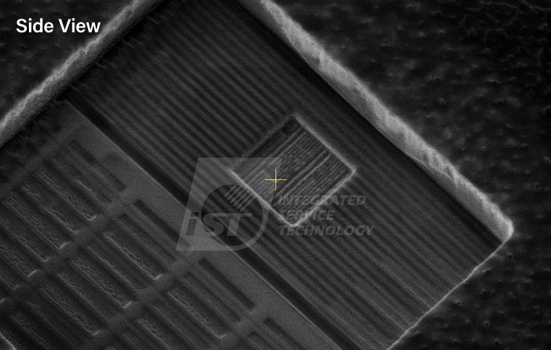
Figure 13: High-Resolution Image at 1.2 pA Low Beam Current, Clearly Distinguishing the M1 Metal Layer at the 5nm Node
(Source: iST)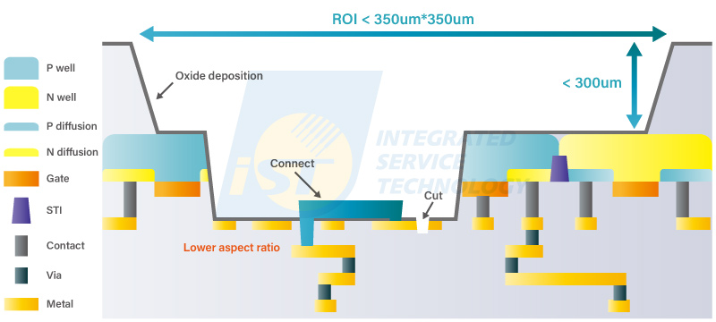
Figure 14: Cross-Section Diagram of FIB Backside Circuit Edit Technology
(Source: iST)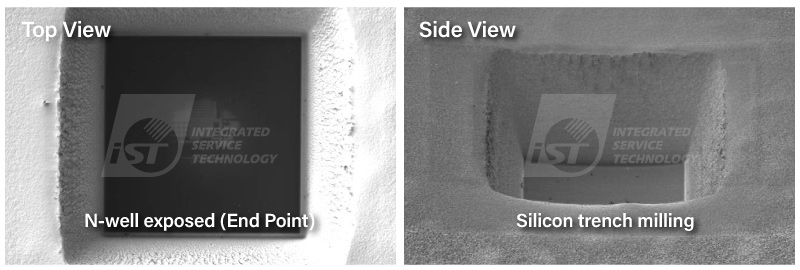
Figure 15: Backside Silicon Trench Etching
(Source: iST)
Figure 16: Advantages of FIB Backside Circuit Edit – Low Aspect Ratio (Left) and Simplified Circuit Modification from the Source (Right)
(Source: iST)(6) Applications of FIB in Various Packaging Types
iST’s FIB Lab can accommodate FIB circuit edits for most of the popular packaging types in the market. Below is an analysis of three specific packaging types.
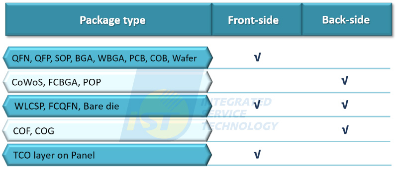
Table 2: Packaging Types Supported by iST’s FIB Lab
(Source: iST)1. WLCSP (Wafer-Level Chip Scale Package)
Since 2014, iST has been providing comprehensive solutions for WLCSP. In addition to enabling circuit edits at both Site-1 and Site-2, iST offers localized solder ball removal and replanting solutions for Site-3, addressing the challenge of performing FIB circuit edits beneath solder balls. Simultaneously, iST supports FIB backside circuit edits and has successfully demonstrated cases of performing both front-side and backside circuit edits on the same sample.
Since its introduction in 2014, iST has executed over 10,000 WLCSP circuit edits for global clients.
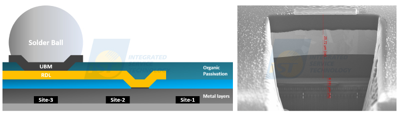
Figure 17: WLCSP Structure and Redistribution Layer Thickness Diagram
(Source: iST)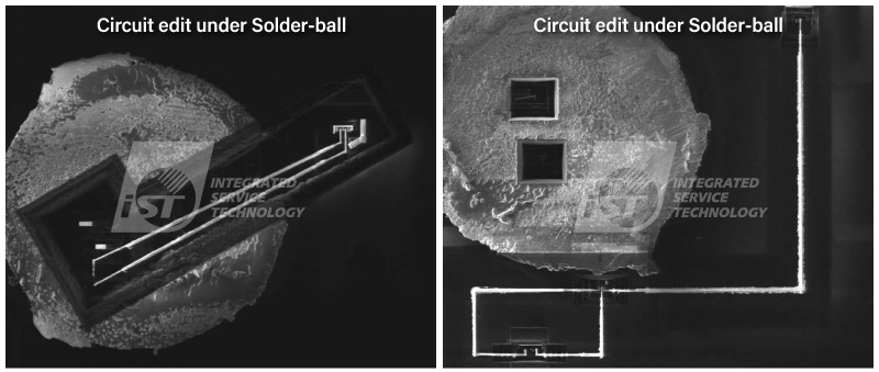
Figure 18: FIB Circuit Edit Performed After Solder Ball Removal, Followed by Re-balling
(Source: iST)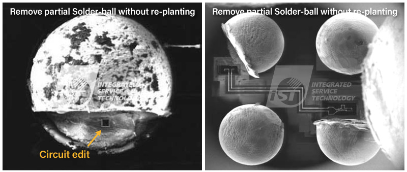
Figure 19: Localized Solder Ball Removal for FIB Edits, Enabling Direct Socketing or PCB Testing Without Re-balling
(Source: iST)2. FCOL (Flip Chip on Lead)
FCOL packaging technology replaces traditional wire bonding with copper pillars and lead frames, reducing package size while lowering thermal and electrical resistance. This enhances both heat dissipation and electrical performance. However, the large lead frames on the chip surface pose challenges for FIB circuit edits. When the target area is covered by the lead frame, FIB modifications cannot be performed.
To address this issue, iST introduced an innovative solution in 2014, enabling localized removal of the lead frame while maintaining the IC’s normal electrical functionality. This approach allows FIB circuit edits to be completed successfully. However, the exposed lead frame becomes more fragile after removal of encapsulation, requiring re-encapsulation to enhance structural stability. It’s important to note that once a lead frame is removed, it cannot be restored, a critical consideration for this process.
For FCOL packages, iST’s FIB Lab also provides backside circuit edit services. Notably, iST has successfully demonstrated cases where both front-side and backside circuit edits were performed on the same sample.
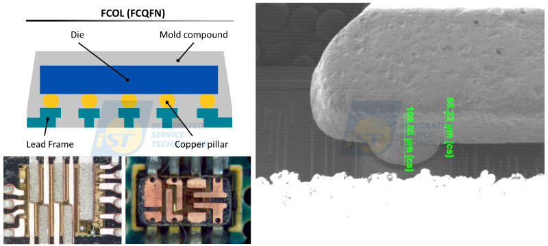
Figure 20: FCOL Packaging Diagram and Chip Covered by Lead Frame After Encapsulation Removal
(Source: iST)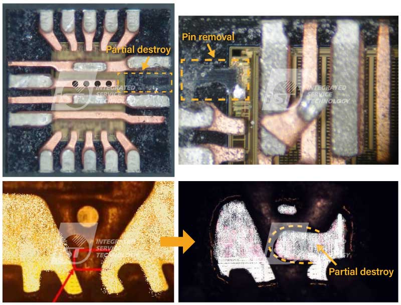
Figure 21: Case Study of Localized Lead Frame Removal
(Source: iST)3. CoWoS(Chip-on-Wafer-on-Substrate)
In recent years, CoWoS has undoubtedly become one of the most prominent packaging technologies. Can this packaging type accommodate FIB circuit edits? The answer is a resounding yes!
As shown in the structural diagram, CoWoS adopts a 2.5D packaging format. The front side of the ASIC chip connects to the substrate through TSV (Through-Silicon Via), while the ASIC chip’s backside remains exposed, allowing FIB circuit edits to be performed from the backside.
However, before performing FIB modifications, the chip backside typically requires thinning through grinding. Traditionally, this process involves grinding the entire backside, which risks damaging the high-bandwidth memory (HBM). iST offers localized grinding for FIB target areas, not only protecting the HBM but also creating the necessary space for subsequent FIB operations.
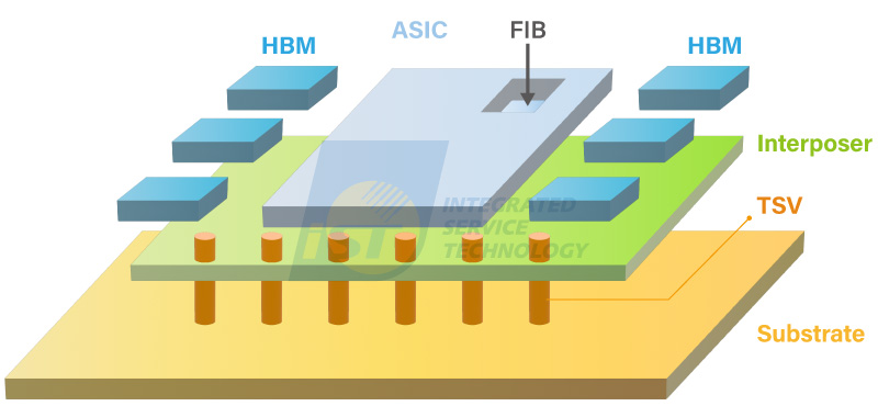
Figure 22: iST Performs Localized Grinding for Target Areas Without Damaging HBM, Followed by FIB Circuit Edit
(Source: iST)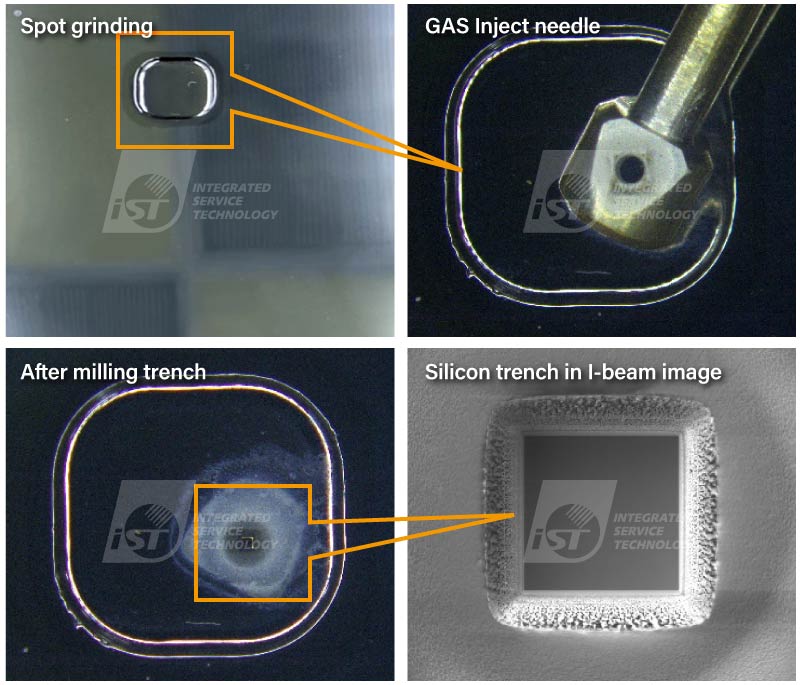
Figure 23: Localized Backside Grinding on Target Areas Followed by Silicon Trench Etching Using FIB
(Source: iST)- Low Impedance Solution
iST is a Taiwan’s first private laboratory to perform FIB circuit edits. Over the past 30 years, iST has successfully resolved countless challenges for its clients, from simple 1L1C circuit edits to addressing complex circuit issues. Whether it involves single-site FIB edits or multi-site failure analysis (FA) across 3–4 testing methods, iST delivers tailored solutions to meet diverse needs.
In 2018, iST became the first to offer backside circuit edit services for 7nm process chips. By early 2021, it had successfully demonstrated backside circuit edits for 5nm process chips. By the end of 2023, iST achieved another milestone by completing a 3nm chip circuit edit case, helping clients quickly identify circuit defects, reduce development time and costs, and accelerate time-to-market for their products.
iST’s FIB circuit editing has consistently maintained a leading position across various process nodes, making it the go-to partner for numerous IC design houses. Furthermore, iST integrates its one-stop solutions for failure analysis and material analysis with 30 years of extensive big data experience. This combination empowers IC designers to tackle the most challenging chip debugging issues with ease and efficiency.
We are grateful for your ongoing support and are pleased to share our expertise in this article. For inquiries, please contact Mr. Wang at +886-3-5799909 ext. 6000
Email: web_fib@istgroup.com;marketing_tw@istgroup.com